This Crucial WBG Power Transistor Reliability Test is Often Missing
By Ron Barr, Vice President of Quality and Reliability, Transphorm
There is a great deal of activity in wide bandgap (WBG) power electronics lately, with Gallium Nitride (GaN) and Silicon Carbide (SiC) devices getting a lot of attention due to the technologies’ superior performance that enables smaller and more efficient power supplies. As device reliability is a key consideration when deciding to design in WBG solutions, suppliers are generating reams of qualification data to demonstrate their products’ reliability. You can now find data on JEDEC and AEC-Q101 product qualification, acceleration factors and lifetime testing for most if not all WBG power transistors on the market.
Conspicuously, however, there is one very important test that is missing from nearly every supplier’s suite of reliability tests: Early Life Failure. This article will discuss what this test is and why it is important. It will also speculate as to why it seems to be missing from most GaN and SiC suppliers’ reliability reports.
Its omission matters.
Regrettably, some suppliers publish data that does not make the distinction between device lifetime and early life failures—polar opposite metrics that sound similar but convey very different information. As such, customers may not know they are missing crucial data that they should have before building their end products.
Figure 1: The bathtub curve demonstrates the failures that, collectively, indicate a devices total reliability.
ELF: What It Is
Early Life Failure (ELF) testing is part of JEDEC’s JESD47K qualification standard1 and is routinely published by producers of Silicon (Si) devices. As a GaN device manufacturer, Transphorm has followed the Si industry’s common practice and has published this data for years—most recently in October 2020—along with details about the methodology used. Virtually no other GaN or SiC supplier has followed suit.
A detailed description of how to run this test is beyond the scope of this article, but here is a quick summary. A large sample of devices are stressed under high voltage and/or temperature for an extended period of time. The entire sample is normally stressed under a single set of conditions (much like a qualification test). Typically, no parts fail during this test.
By applying the appropriate acceleration factor to the data, we are able to calculate the number of accelerated use hours. By next applying the appropriate statistics, we can calculate a quality level that is usually expressed in failures per billion device hours (FITs) or parts per million per year (PPM/Year). For those who want to gain a detailed understand as to how this test should be run, please refer to the JESD74A test standard2.
Typically, billions of accelerated device hours over hundreds or thousands of devices can be required to generate the appropriate statistics. For example, Transphorm’s Gen III platform ELF test used 2,000 devices sampled from 30 product lots for 500 hours at 800 volts to develop the necessary statistics.
In contrast, a device lifetime test (the test most often confused with ELF) can be conducted with as few as 120 devices with a high degree of confidence. Lifetime data is sometimes inappropriately expressed in FITs, which is misleading and can cause that customer confusion. FITs are only used during the “flat part" of the bathtub curve, as the unit assumes a constant failure rate. More importantly, the FIT rate is supposed to be addressing the risk of a device failing in the first few years, not its ultimate lifetime due to wearout.
ELF: Why It Matters
Early Life Failure testing is a quality test. It addresses the risk that one will experience a product failure in the field before hitting the intrinsic lifetime of the device. It is an important tool for managing the warranty risk of a product in the field. To understand why a product may fail before it reaches its intrinsic lifetime, we must descend into the deepest, darkest crypts of the semiconductor wafer fab and uncover its biggest secrets.
Secret 1: Wafer fab processes have defects, and these defects can make it out of the wafer fab.
Silicon, GaN and SiC processes have defects. Resist residues, stringers, voids, pinholes, corrosion spots, delamination and particles, particles, and more particles. Some of these defects are common to all semiconductor processes and some are particular to GaN and SiC WBG materials. The management of defects consumes a large portion of the engineering talent of any semiconductor wafer fab and captures significant capex dollars for equipment to inspect and identify those defects. Interestingly, one of the world’s largest producers of semiconductor capex equipment gets the bulk of its revenue from defect inspection equipment (which the author knows quite well as having worked there for the better part of a decade).
In the world of defect inspection, there are three types of defects that the wafer fab engineer must confront:
1. Killer Defects that cause device failure during either wafer probe or final tests.
2. Nuisance Defects that show up on the inspection equipment, but functionally have no effect.
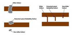
3. Latent Defects that make it through test but cause early life failures. (In other words: a latent defect is a defect that does NOT cause a test failure but CAN cause a failure in the field.)
“Experiments conducted at multiple device manufacturers have shown that for every 100 killer defects that cause yield loss, there are approximately 1-2 latent defects that will result in a reliability failure. This relationship between killer and latent defects is unequivocal and applies to a broad spectrum of defect types.”3
Which leads us to…
Figure 2: The diagram indicates where the three types of defects might exist in a semiconductor device pattern. It shows particles potentially interrupting current flow on the left or inadvertent connections between two current paths on the right.4
Secret 2: The lower the yield, the greater the risk of a Latent Defect getting out of the wafer fab.
While testing, screening and inspections can reduce the reliability risk, ultimately high yielding stable processes are key. Poor probe yields are an early indicator of possible early failures in the field.
Early Life Failure testing is a definitive method for “checking” how well all these processes are doing by placing a statistically significant sample of devices under high stress conditions and employing the appropriate acceleration models. The tests themselves are not difficult to run. Customers should be looking for their WBG suppliers to generate this data. As noted earlier, offering this data is a common practice of Si suppliers. And, again, as mentioned already, lifetime data can be easily confused with early life data…causing the risk for early failures to go undefined, which in turn can translate into field failures as devices with Latent Defects wind up out in the field.
Understanding the Industry’s Inconsistency
So, why is it that Transphorm publishes ELF data while other GaN and SiC device makers do not? While this question needs to be asked of the actual suppliers, some speculative reasons follow:
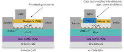
1. Transphorm utilizes what is known as a d-mode HEMT, where many other GaN suppliers have designed-in the e-mode HEMT. The process of producing an e-mode device requires complex etching and deposition processes that directly involve and impact the gate structure. To create the gate structure of an e-mode device, a recess is etched into the layers above the GaN layer with a gate deposited on top. The d-mode device does not have this etch step and the gate metal is deposited on a “pristine” gate dielectric layer. The etching and deposition process in the gate region of an e-mode device can generate a number of different types of defects that could possibly not be screened out via electrical probe and test. Defects in the gate region are especially problematic with respect to ELF reliability as this is a region under high electric field and sensitive dielectric layers. The d-mode device, because of its simplified structure and clean process, is far less vulnerable to Latent Defects in the gate region and inherently has a lower early life failure risk. This lowered risk is supported by extensive early life failure data that show very low potential FIT rates and excellent field reliability of Transphorm’s products.
Figure 3: Cross-section analysis of the d-mode HEMT and an e-mode p-GaN FET show how device construction can, in the case of e-mode, affect the gate integrity when compared to that of a d-mode HEMT.
2. Transphorm’s GaN epitaxial growth process has distinct advantages over that of its SiC competitors. GaN is a mature technology that has been used for many years in LED production RF GaN and power GaN devices. The starting material for Transphorm’s GaN is a Si wafer, which is probably the most “perfect” semiconductor material available to industry. The processes of growing SiC wafers and SiC epitaxial layers are fundamentally different from the same Si processes; they offer unique challenges in controlling defects. “Silicon carbide is not defect-free; actually, compared with silicon, it’s a highly defective material.”5 Transphorm has demonstrated probe yields that are comparable to standard CMOS, which indicates that defects from GaN EPI are not much different than those of Si EPI. High yielding processes tend to produce improved ELF results.
3. Transphorm is fully vertically integrated and has ownership and control of the entire process from device design and GaN epitaxial growth through to wafer fabrication, probe, assembly and test. Devices are designed to be compatible with their process capability and optimized accordingly for yield and reliability. A risk for other companies that outsource their manufacturing is a reduced ability to solve process problems and optimize their designs. Their troubleshooting occurs between the various silos in their supply chains, which complicates the process. Once a weak design and process has been released to the world, one cannot test and screen their way to a reliable product.
The suppliers of WBG devices owe it to their customers to perform complete product qualification prior to going into mass production so that customers can manage their ELF risks effectively. JEDEC and AEC qualification requires this testing and device manufacturers should be supplying the data. Purchasing agents should demand ELF data and engineers as well as QA personnel should be skeptical when lifetime data is presented as a substitute. Focus on ELF is an overall win for the GaN industry as it accurately validates the reliability of the devices themselves, in turn helping the technology’s adoption.


