The pressures to move swiftly from the design phase to functioning hardware are at the core of every product development cycle. The integration of test equipment with a design automation tool helps to streamline RF circuit design.
This capability makes it possible to do things like directly correlate simulation and prototype data, create virtual hardware, simulate difficult-to-reproduce hardware impairments, and extend test-equipment capabilities. Tying together an electronic design automation (EDA) tool with measurement and analysis instrumentation provides a number of new benefits for accelerating design.
To demonstrate these connected solutions, we will use Agilent’s Advanced Design System (ADS) and Vector Signal Analyzer (VSA) as examples. The ADS is a high-frequency, mixed-signal design environment that harnesses a variety of tools. Instead of putting a standard set of ICs and discrete components onto a circuit board for modeling, the ADS performs a functional simulation of the board’s components with RF impairments in place. The VSA tracks the magnitude and phase of the input signal.
Linking a Design Environment With a Signal Analyzer
Before discussing specific design scenarios, let’s examine the ADS, the VSA, and how they can be linked together. The block identified as CAD in Figure 1 is the design environment in which simulation occurs. It could be, in fact, almost any type of EDA tool. Its role is to enable designers to develop transmitters, receivers, or virtually any set of RF components and subsystems.
The ADS models simple linear parameters, such as resistances and capacitances as well as very complex functions such as high-frequency loss and transmission-line properties. On the signal-processing side, the ADS simulates fixed- and floating-point designs and verifies many of today’s communications protocols. It offers an environment that can model both protocol and real RF performance in the presence of various impairments.
Once the initial design has been completed, data from the simulation can be streamed to a signal analyzer as denoted by the simulation arrow in Figure 1a. Data is ported from the simulation environment in the designer’s PC, where the EDA software is resident, to the VSA software present in the same PC.
In effect, the VSA software is the brains of the analyzer. It operates in a Microsoft Windows environment. The software can put a number of built-in analysis tools to work, such as examining the data in the time and frequency domains.
In addition to parameter measurements that you would expect a spectrum analyzer to perform, the VSA possesses analog and digital demodulation capabilities compatible with numerous advanced signal characteristics. Therefore, the designer can troubleshoot problems in the transmitted signals rather than just recognize they exist, as with a bit error rate (BER) test that simply is a pass/fail test. Since the VSA offers the capability to look at other aspects of testing, such as error vector magnitude (EVM), it can help localize sources of an unacceptable BER in a design.
Fine-Tuning the Design
Once the software has analyzed the signal, the results of the simulation and VSA analysis are streamed back to the EDA tool for tweaking, correcting, and enhancing the design. This is denoted by the line returning the CAD in Figure 1a identified as measure performance.
Now let’s consider a scenario where the EDA tool and the signal analyzer have gone through a number of iterations. Now it is time to take what appears to be a pretty good design resident in the EDA environment and stream these signals into the real world for testing, as depicted in Figure 1b.
Before ever building any of the hardware, we can stream the output signals from our design into an arbitrary waveform generator to actually create the signals of interest. In turn, the signal generator can output the signal (baseband or RF) to the real world, up converting as necessary so that the signal can be sent to the actual hardware.
Now the measured response can be taken from real hardware, as denoted in Figure 1b, and fed back to the signal-generator software. Finally, we can port the design data back to any destination we choose, as denoted by the three arrows exiting from the signal-analyzer software in Figure 1c.
To summarize, we have an environment in which we can bring together simulation analysis and actual DUT performance with the same set of tools. This means the designer can compare the measured results directly with the simulated results.
More Vantage Points
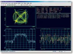
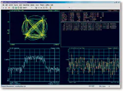
The VSA application could be configured to show several different windows, from a single pane to all four as shown. In the top left pane is a constellation diagram. The red dots are symbol points; the green lines interconnecting them are the trajectories from one symbol location to the next. Here the designer has a time-domain view of the instantaneous phase and magnitude of the output from the I-Q demodulator in the VSA domain. The red dots are positioned according to the modulation format.
In the lower left, the blue diagram is the spectrum of the modulated signal being measured. It is comparable to what you would obtain with a spectrum analyzer.
The error signal summary table on the top right-hand side shows the essential parameters that are being captured and identified with regard to the signal of interest. The chart is divided into sections. At the top is the summary of error results such as the EVM percentage as an rms value, the peak magnitude, and the phase of the EVM. I-Q error, frequency error, and several other measurement results also are displayed in the summary table.
The section in the middle contains the actual bits that have been demodulated from the signal. Now we are looking at the spectrum being measured, its constellation, and its demodulated contents all at the same time. At the bottom right is a plot of the error vector magnitude vs. time. The red dots correspond to the symbol times clocked in and displayed in the constellation diagram.
The EVM trace is a continuous measurement of the difference between the measured signal and a reference signal generated by the VSA. The reference signal generation is based primarily on the span, center frequency, modulation format, symbol rate, filter parameters, and the input signal.
The yellow trace tells you what the error signal looks like plotted against time. The red dots correspond to the same symbol points as we see in the constellation diagram. With this trace, a designer can perform additional analysis, perhaps evaluating the frequency content of the error signal.
Such analysis can help identify a number of problems. For example, if these error components are deterministic, then they will show up in the EVM spectrum. Measuring the spectrum can give added insight into the nature and origin of these error signals.
The Benefits of Simplification
Frequently, a variety of tools is used in the design and development process. In such cases, simulation occurs in one environment with one particular type of EDA tool. Then the hardware is assembled, and the focus shifts to making the hardware behave like the EDA tool.
But if measurement tools used to evaluate the hardware are not the same as those used to evaluate the simulation, the designer can wind up with differences that are difficult to resolve. Testing the hardware with the same tools that tested the software model makes sense. Since there is no difference between analysis methods for simulation and prototyping, someone unfamiliar with the ADS or the VSA only needs to learn one tool to analyze digital communications systems.
It is the ready interchangeability of simulation with hardware realization that serves as the basis for a number of scenarios that become possible with the EDA tool/instrumentation link. For more information, see the sidebar “EDA Tool/Instrumentation Links—Three Scenarios.” (see below)
EDA Tool/Instrumentation Links
Three Scenarios
Supplying a Missing Link
A new transmitter/receiver design is broken up into a set of tasks and assigned to various engineering teams. The simulations are completed, and the go-ahead for prototyping is given. As a result, the call goes out to begin collecting sample components for assembling the subsystems of the complete transmitter/receiver chain.
But one section in the middle has a problem. It might be some type of a filter that is near the middle of the design. Without that, you can’t fully test the hardware.
To work around this problem, the design group initiates the following: Using the VSA’s recording capabilities, the signal from the upstream portion of the hardware implementation is captured, brought into the ADS model of the filter, passed back out to a programmable signal source, and finally fed to the hardware version of the remainder of the transmit/receive chain.
Modeling Atmospheric Impairments
A satellite communications company working on a downlink encounters environmental distortion superimposed on the signal, making it difficult to communicate with the satellite. The engineers are not really sure what the problem is. Through testing, they determine that sunspots are creating electromagnetic interference, not something that can be readily simulated with physical components.
They recreate the effects in software, using the ADS to model the signal impairment. The signal is passed through the distortion-inducing model and brought back out. Then, it is fed to the receiver via the programmable generator to see if an equalizer can be designed to compensate for these effects. Finally, the signal is streamed to the hardware using a programmable signal generator.
Filling in for Instrumentation
The cable industry is moving toward a new modulation medium for transmitting through wire lines. It is 1024 quadrature amplitude modulation (QAM), a considerable design challenge because today’s levels are at 256 QAM. The value denotes the number of discrete signal states in the modulation format. But the test equipment essential to make the type of measurements necessary in the subsystems does not yet support this new format.
Because it is an effective digitizer, the VSA could be used to capture the data and bring it into something such as the ADS. Then, within the ADS, the required testing is created in software to perform the demodulation, execute the analysis, and determine characteristics such as EVM. This quantifies any type of modulation errors that the signal exhibits in the course of the design.
About the Author
Brent Forman is a technical consultant for Agilent Technologies, focusing on RF and microwave applications and vector signal analysis and developing customer training for this technology. He received a B.S.E.E. from Rochester Institute of Technology and is working on an M.S.E.E. in DSP and communications at Northeastern University. Agilent Technologies, 40 Shattuck Rd., Andover, MA 01810, 978-681-2162, e-mail: [email protected]
FOR MORE INFORMATION
on software-based EDA tools
www.rsleads.com/308ee-176
Return to EE Home Page
Published by EE-Evaluation Engineering
All contents © 2003 Nelson Publishing Inc.
No reprint, distribution, or reuse in any medium is permitted
without the express written consent of the publisher.
August 2003
About the Author
Voice Your Opinion!
To join the conversation, and become an exclusive member of Electronic Design, create an account today!

Leaders relevant to this article:

