Loaded board testing pays for itself by reducing field returns and bone-pile scrap.
You seldom read an article about PCBs or semiconductors without encountering test-related phrases and acronyms. Cost of test, multisite testing, functional test (FT), in-circuit test (ICT), built-in self-test (BIST), low-cost test, boundary scan, design for test (DFT), and similar terms are hot items these days.
Increased awareness of the importance of loaded-board test has occurred partly because of the economic realities of intense competition. Test costs must be low, but simply reducing the amount of testing, such as by doing lot sampling, may not be appropriate. Thorough PCB testing as early as possible in the production process can be a better choice because it reduces very expensive field failures.
Other factors such as increased component density, very high component quality, and the desire to verify a board's performance in the field also have prompted manufacturers to reconsider long-established test paradigms. For instance, it may be sufficient to confirm component type and orientation rather than perform a comprehensive component test. If so, perhaps a low-cost manufacturing defect analyzer (MDA) can be used instead of expensive ICT ATE.
It may be feasible to replace at least part of a high-cost FT stage with some form of BIST. Or perhaps BIST is required because complex parts such as microprocessors can be tested most easily in this way. Board-level BIST marginally increases the bill of material costs. But this can be offset by reduced test time and, in the case of boundary scan testing, the capability to program devices in situ. Additionally, the performance of a board with BIST can be confirmed in the field, a valuable benefit when troubleshooting complex equipment problems.
Common to all these considerations is the role of the test fixture. Both ICT and MDA require access to each component or small cluster of components so a bed-of-nails fixture is needed. In addition, FT can provide more detailed fault analysis if access to internal nodes is provided by this type of fixture.
Bed-of-Nails Test Fixtures
For many years, vacuum-actuated wired fixtures were the norm. All testing was performed from the underside of the board. This meant that the operator had very good access. The board simply was positioned correctly and a vacuum applied to pull it down against the test pins. The board design included accurately positioned guide-pin holes and sufficient area around the perimeter so a good vacuum seal could be made.
Actually, applying a vacuum beneath the board allows atmospheric pressure to push the board down from the top. Using a vacuum in this way applies a uniform pressure over the entire board surface and is particularly well-suited to large boards. Small boards can be tested in multiples, or if tested separately, the smaller fixture can use mechanical or pneumatic actuation to avoid the cost of a vacuum system.
However, things become more complicated if additional pressure is needed to cope with a concentration of test pins in one area. Hold-down gates with mechanical posts or beams are required to force the board down against the spring-loaded test pins in areas where atmospheric pressure alone is not sufficient.
In addition, today more boards require both topside and underside probing than in the past. This may be due to component density, but top access also is required for testing the color and brightness of LEDs, verifying the presence of connectors, optically recognizing part polarity, and ensuring continuity through vectorless test. For these reasons, the traditional vacuum fixture does not offer a quick load/unload advantage in all situations.
Providing an overview of the test fixture market, Bill Oxley, senior director of sales at IDI Test Products Group, observed, “There are companies that specialize in a certain type of test fixture. The largest business segment, about 70% of the total market, is in wired, vacuum-actuated, single-sided ICT fixtures. Wired, pressure- and manually actuated, single-sided fixtures for MDA testing represent the next largest at 20%. Wireless ICT makes up about 5% of the total market and is experiencing a slight surge in popularity.”
The apparently contradictory information provided by several companies confirms specialization within the industry. For example, in the last 10 years, CheckSum's fixturing division has experienced a very large change in customer preference from vacuum to pneumatic actuation.
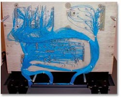
Ken Hallmen, CheckSum's marketing manager, explained that the maintenance and expense associated with a vacuum system were not justified once the quick board load/unload capability was lost. By using an array of pressure rods, a pneumatic fixture can uniformly apply the required force at a lower cost. Figure 1 shows the internal wiring of a typical CheckSum MDA fixture.
Courtesy of CheckSum
Richard Caley, owner of Quality One Test Fixtures, commented that the so-called vacuum-lid or vacuum-cover type of fixture was coming back into fashion. Rather than establish a vacuum beneath a board, something that can be difficult if the board has cutouts or open vias, a vacuum lid fits over the board assembly and seals to the surface of the test fixture. When a vacuum is applied, the lid's integral mechanical gates press down against the board.
“Two factors are responsible for the resurrection of the vacuum-lid fixture: price and PCB flatness,” Mr. Caley said. “Vacuum lids lost popularity years ago because they prevented topside access to the board during test. At that time, large pin-counts and control of PCB flexure were driving an increase in pneumatic fixturing. But, vacuum-lid is a good, low-cost solution to large pin-counts as long as access to the PCB during test is not required. About 50% of the fixtures we make are the vacuum-lid type.”
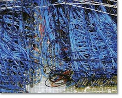
Also in the vacuum-actuation camp is UNI-FIX. Gary Oleksiak, the company's president, said that 80% of its ICT fixtures are vacuum actuated with mechanical gates, while only 10% are traditional molded-seal vacuum types. He estimated that as much as 30% of the ICT fixtures are wireless with 70% being conventional wired types. Figure 2 shows typical point-to-point wiring in an Agilent Technologies short-wire ICT fixture.
Courtesy of UNI-FIX
So-called wireless or no-wire fixtures use a custom PCB to replace the large amount of wiring characteristic of traditional fixtures. This technology can be very cost-effective but hasn t been widely adopted as a general solution. However, where signal integrity is important, the number of test points is high, and especially if several copies of the fixture are required, wireless fixtures can save money.
As with the type of actuation, the popularity of wireless fixtures varied greatly depending on a company's experience. “There is a crossover point where wireless fixtures may become more cost-effective,” Mr. Oleksiak explained. “A 200-point wireless fixture may cost 15% to 20% more than a wired counterpart, but if multiple units are required, the wireless approach becomes more attractive. Cost and lead-time savings can be seen on just one large fixture. Even with the cost of producing the fixture-interface PCB, a 2,000-point wireless fixture will cost 15% to 20% less than a wired fixture.”
Other manufacturers didn't see the same economies in wireless fixturing. For example, Gary St. Onge, president of the Everett Charles Test Fixtures Group, said, “It is still cheaper to use a $10/h wire wrapper to wire a fixture than to design, manufacture, and test a one-of-a-kind wireless PCB. Customers that have been most successful with wireless fixtures generally manufacture their own PCB, which then is supplied to the fixture company for integration.”
IDI's Mr. Oxley explained the technical advantages of wireless fixtures: “When used in conjunction with geophysical nail-locating software, the trace lengths on the multilayer translator boards used in wireless fixtures can be minimized to less than 3 inches. Also, controlled impedance circuits can be introduced and on-board circuitry added in the fixture to improve performance.”
Other benefits include elimination of blocked resources on the tester interface and the possibility of avoiding a high concentration of tightly spaced probes. In addition, especially in fixtures with high pin-counts, this technique obviously eliminates the thousands of wires that otherwise must fit in a small enclosure.
DFT Considerations
Successful test-fixture operation depends on maintaining accurate probe positioning during repeated contact to production quantities of UUTs. Although this is entirely a mechanical engineering problem, many aspects of both the fixture and the UUT design affect performance.
UUT Size
The larger a PCB, the more difficult it is to maintain its flatness. Also, a large board will likely contain more circuit nets and require a greater number of probes. Both board warping and the spring pressure resulting from a high probe count can be overcome with sufficient force.
Mr. Caley of Quality One Test Fixturing observed that high pin-count and the need to control PCB flexing drove the increase in pneumatic fixtures a few years ago. However, in his experience, vacuum-lid fixtures also can provide the necessary actuating force and are a lower cost solution. Neither pneumatic nor vacuum-lid fixtures allow board access during test.
The uniform distribution of circuitry on a PCB may not be achievable because of electrical signal constraints, but mechanically it is desirable. A relatively low and constant test-probe density over the UUT area results in a simple gate structure and uniform application of the actuating force.
Electrical Net Density
In cases where high probe density is required, subminiature probes must be used. Probes that can be placed on 0.008″ centers are available although 0.1″, 0.05″, and 0.039″ center-to-center dimensions are more common.
Very small probes are fragile and may require a separate guideplate to ensure accurate tip positioning. In addition, high probe density results in locally high spring pressure that must be offset by a substantial gating force. These types of constraints are routinely overcome in production test-fixture designs but at higher cost and with reduced reliability compared to a fixture for a UUT designed to allow more uniform spacing of larger, robust probes.
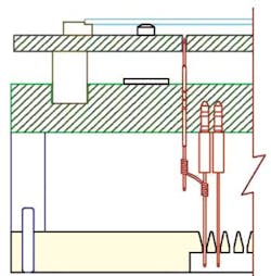
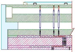
A locally high concentration of probes also affects the internal fixture elements. The bodies of the test probes or probe receptacles are press-fit into a thick insulating sheet called the probe plate. The probe plate provides the reaction force at the bottom of the probe spring, and dense concentrations of probes will cause the plate to deflect downward in use. The relationship of the test pins, personality pins, a probe plate, and a guide plate in an Agilent short-wire fixture is shown in Figure 3a.
Courtesy of UNI-FIX
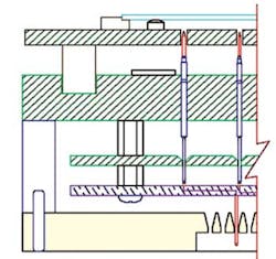
In a wired fixture, probe plate deflection only affects positioning of the probe tip against the UUT. However, because double-ended pogo pins typically are used in a wireless fixture, high spring forces also may deflect the custom interface PCB. This PCB replaces the wiring in a conventional test fixture and is mounted to the underside of the probe plate (Figure 3b).
Several techniques reduce or eliminate the resulting deterioration of the lower pogo pin-to-interface board contact integrity. For example, Agilent Technologies• Deflection Analysis Software automatically finds the best locations for mechanical fasteners and minimizes their number. It analyzes the interface board layout to find the maximum point of deflection, adds a mechanical fastener to the probe plate, and repeats the process until deflection over the entire PCB is <0.01".
An alternative to traditional wireless fixturing is available in the Genesis Printed Wire Fixturing System developed by UNI-FIX and Schein Research. Rather than double-ended pogo contacts, the Genesis system uses a specially designed Z-Force• Receptacle that provides a sliding contact for the tail of a conventional single-ended probe.
As shown in Figure 3c, the interface board is fastened directly to the underside of a so-called Z-plate. This is a thick insulating sheet into which holes have been drilled to accept the probe tails and counterbored from the bottom to house the Z-Force Receptacles and small springs.
Fastening the interface board to the bottom of the Z-plate compresses the springs and establishes contact to all the receptacles while trapping them in their drilled cav-ities. Because of the sliding contact, little if any of the probe-plate deflection is transmitted to the interface board via the receptacles.
Problems similar to those caused by a high concentration of test probes also may be experienced in conventional wired fixtures that have a large number of personality pins. A paper from the Hewlett-Packard Manufacturing Test Division, High Node Count Fixturing Solutions for HP Short-Wire Test Fixtures, specifically addressed the upward doming of the probe plate caused by a fixture's many personality pins contacting the HP 3070 Tester's system interface pins. In extreme cases, a probe tip may miss its intended target when the fixture is actuated.
A very straightforward solution, also applicable to probe-plate flexing caused by highly concentrated UUT probes, uses a thicker plate. Sometimes a second plate is bonded to the standard-thickness plate. Drawbacks include the increased difficulty of accurately drilling mounting holes in a thick plate for small-diameter probes.
Alternatively, a two-plate solution is suggested, which eliminates the UUT probe pointing errors caused by personality pin-induced bowing. In this arrangement, the probes are mounted in the upper plate as usual. However, the personality pins are mounted in a separate lower plate that has clearance holes for the probe tails. The plates are spaced about 0.05″ apart and connected together only around the perimeter. This construction concentrates the deflection caused by the personality pins in the lower plate, effectively stopping transfer of this force to the probe plate.
Signal Integrity
Wired fixtures work well with low-frequency signals, but the positioning and length of the wires result in unpredictable crosstalk and signal distortion at higher frequencies. If only a few fast signals are involved, twisted-pair wiring or coaxial cables can be used within a conventional wired fixture.
However, if the integrity of many signals is important, then a wireless fixture is a much better solution. Controlled impedance traces can be designed into the fixture's interface board. In addition, much lower inductance power and ground distribution will significantly reduce ground bounce. This phenomenon often is associated with boundary scan testing because of the large transient currents caused by the simultaneous switching of many device outputs.
Summary
As PCBs become more complex and circuit density increases, adoption of DFT techniques is mandatory. Only if the design engineer understands how a board will be tested as well as its intended function can he produce the optimum result.
In some cases, the need for certain test-fixture characteristics is obvious. For example, a shielded fixture such as the Rohde & Schwarz TS7110 is necessary if the RF circuitry on a PCB will be tested along with other lower speed circuitry. Similarly, a wireless fixture is better suited to boundary scan testing than a wired fixture.
On the other hand, all of the companies that contributed to this article agreed that the selection of a fixture technology was driven largely by cost. So, it's not surprising that conventional wired fixtures remain by far the largest market segment. Their construction has become standardized and automated to the extent that users can expect to receive a completed fixture within five days of providing the board information.
Nevertheless, a range of actuation methods and fixture technologies is available because board test is not a one-size-fits-all proposition. Especially if your application involves thousands of probes, boundary scan testing, multiple test stations, or high-speed signals, you need to consider the overall cost of test. In the long run, a low-cost fixture may be the wrong choice if poor signal integrity leads to false failures or a large number of escaped faults that cause customer dissatisfaction.
Is the need for a test fixture going to be eliminated soon? Not likely. In spite of predictions that BIST techniques eventually may be all that's needed, the reality is very different today.
CheckSum's Mr. Hallmen, commented, “In our experience, boundary scan is talked about more than it gets used in actual applications. Most frequently, it is used for part programming or perhaps to test a device that has an integral boundary scan port, but seldom do we see entire scan chains built into commercial products.”
FOR MORE INFORMATION
on bed-of-nails test fixtures
www.rsleads.com/403ee-183
www.rsleads.com/403ee-184
www.rsleads.com/403ee-185
on competitive quotes for a fixture
www.rsleads.com/403ee-186
on MDA testers and fixtures
www.rsleads.com/403ee-187
About the Author
Voice Your Opinion!
To join the conversation, and become an exclusive member of Electronic Design, create an account today!

Leaders relevant to this article:

