The current shift in the test methodologies is away from the ubiquitous single stuck-at fault model.
The best test for any device is to exhaustively test the device. The quality of such a test would be perfect since any defective IC would be identified, and all the shipped ICs would be defect free.
However, test resources are limited by the tester memory, the test application time, and the time to generate the test suite. As a result, exhaustive testing is not a viable test solution. The alternative would be to itemize all the defect mechanisms and categorize them according to their probability of occurrence.
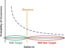
Figure 1 shows a sorted list of defects on the X axis. These defects are sorted by their probability of occurrence, where the most probable defect is on the left and the least probable defect is on the right. Because of limited resources, a partitioning of the defects is performed where a subset of the defects is targeted for creation and application of test patterns.
Figure 1. Defect Categorization for Testing With Limited Resources
This figure gives an idealistic view because resources are most efficiently used if the most probable defects are targeted. The quality of the test set is maximized in this scenario.
While the presentation in Figure 1 may seem quite logical, the requirement to list the defects is unrealistic. Defects can manifest themselves in too many ways, affecting a large part of the silicon or only small locations on the silicon.
When they affect small locations, they are called spot defects. These spot defects are extra or missing material in the IC that may occur in any of the many steps in the IC manufacturing process.
Spot defects are the primary target for test since these are much harder to detect than defects that affect a large part of the silicon. Instead of listing these defects, abstract representations of the defects, or faults, are used. The faults guide the test creation and evaluation to areas in the design where the defects are located.
Clearly, the fault-abstraction process is an important factor in the quality of the tests created. Today, the single stuck-at fault model is most commonly used.
Is Stuck-At the Right Target Fault Model for Test?
Defects in TTL that occurred during manufacturing behaved like stuck-at faults, so using single stuck-at faults to guide automatic test pattern generation (ATPG) and fault simulation worked very well. Tools matured around this concept where scan technology developed to make the task of generating the tests much easier. All these methods were fine-tuned to the single stuck-at fault model.
Over time, the industry has become accustomed to the benefits of the single stuck-at fault model:
-
Easy to describe and represent.
-
Limited number of target faults.
-
Evenly distributed tests across the design/IC.
The industry appreciates these benefits so much that it has not broadly adopted the many additional fault models that have been developed over the years, such as bridging, transition, stuck-open, path-delay, and N-detect faults.
Technology has moved from TTL to CMOS to future technologies that will address leakage-current issues. The defects are very far from behaving like stuck-at faults.
In most processes today, resistive vias are a predominant problem. These defects impact the timing of the IC and are not detectable by a test generated to detect a stuck-at fault. Like resistive vias, bridges and coupling effects impact the timing of the design, the primary symptom not covered by the stuck-at tests.
Which Faults Do We Test For?
The known fault models that represent or generate timing-sensitive voltage measurements are the path-delay and the transition fault models. The path-delay fault model takes into account the sum of all delays along a path while the transition fault model accounts for localized faults (delays) at the inputs and outputs of each gate.
In a design containing n lines, however, there can be a maximum 2n transition faults (a slow-to-rise and a slow-to-fall fault on each line), but there potentially can be more than n2 (or exponential) path-delay faults. Since all the paths cannot be tested, the path-delay model requires identification and analysis of critical paths in the design. This makes it more complicated to use on large designs. Consequently, the transition fault model has been accepted as a good method to test for delay faults.
Testing for transition faults is similar to that of stuck-at faults in many respects. To test for stuck-at faults, two steps are involved: generate a test vector that excites the fault and propagate the faulty effect to a primary output or a scan flip-flop.
While testing for transition faults, we need to change our approach somewhat. The first step launches a transition. If the fault is a slow-to-rise fault, the second step tests for a corresponding stuck-at-0 fault. And, if the fault is a slow-to-fall fault, the second step tests for a corresponding stuck-at-1 fault.
As easy as it may sound, this requirement introduces its own set of challenges. However, with the help of current-generation ATPG tools, it is becoming easier to model these faults and test for them.
Practicality of Transition Fault Tests
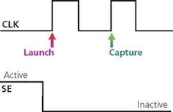
Two techniques can be used to test for transition faults. In the launch-from-capture technique, the first vector of the pair is scanned into the chain, and the second vector is derived as the combinational circuit’s response to the first vector. In this method, the launch and capture operations are performed with the scan-enable signal set to the functional mode. Figure 2a illustrates this approach.
Figure 2a. Launch-From-Capture
Before the launch sequence, the required vectors are shifted into the scan chains. Optionally, a dead cycle can be inserted before the launch pulse to gain better control over the scan-enable signal that must be toggled. The scan-enable then is toggled, and the circuit enters the functional mode. Primary inputs are applied as required, and the scan-enable signal is given enough time to propagate to all flip-flops.
By now, we have set the required values at all flip-flops, meeting the prerequisite to launch a transition. Next, two quick clock pulses with a period corresponding to the functional operating frequency of the circuit are pulsed. The first pulse acts as the launch pulse, and the second pulse captures the effect. We have no control between the launch and capture pulses, and the second vector of the transition test is derived as a combined response to the first.
This operation is followed by the scan-out phase. By following this sequence, the effect of the transition can be observed at the scan-chain end points or at primary outputs.
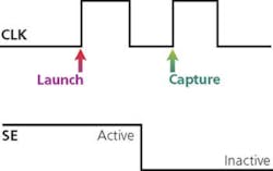
In the launch-from-shift technique, both the first and second vectors of the transition fault test pair are delivered directly through the scan cells themselves, and the transition is caused by the last shift operation. Figure 2b illustrates this approach.
The first vector in the test pair is derived by shifting the scan chain N–1 times where N is the length of the scan chain. With the scan-enable signal set to the shift mode, shifting the scan chain once more generates the second of the two vectors, and this launches the transition. The scan-enable signal then is set to the functional (capture) mode, and this change has to take place at-speed. The effect of the transition is captured into the flip-flops, and the scan chain is shifted out so the effect of the transition can be observed.
The most important difference between the two techniques is the need for at-speed scan-enable operation in the launch-from-shift technique. If an at-speed scan-enable signal must be supported, routing should be done very carefully so the effect of any change from the shift to capture mode can be propagated to all flip-flops in a small window of time. Meeting such strict requirements is not possible all the time, especially at higher frequencies.
Tester interfaces for a low-cost tester, like the one we use at TI, do not support at-speed changes to the scan-enable signal. For example, in a design with a functional frequency of 400 MHz, the low-cost tester only provides a 2.5-ns window to de-assert the scan-enable signal and propagate the effect to all scan cells, which is difficult to achieve.
In addition, the transition-fault ATPG patterns also might require that primary inputs be changed and primary outputs observed. Such requirements also are not supported by low-cost testers. As a result, the launch-from-capture technique has been adopted as a popular method to screen speed-related defects using low-cost test equipment.
DFT Considerations
With such complicated issues at hand, it takes a great deal of planning and execution to model test logic capable of at-speed testing. In addition, we must deal with always-changing design styles and features.
Most designs in the industry operate on multiple clock domains. The key to ATPG is to keep flip-flops in each clock domain chained with other flip-flops in the same domain. It is best not to combine flip-flops from different domains on the same scan chain.
If they have to be combined, lock-up latches must be placed at the boundaries of each clock domain. These lock-up latches eliminate clock skews between domains while shifting through the scan chain. These delay the data for half a clock cycle, from the rising to the falling edge, providing a high tolerance to skew between domains.
False paths in designs can pose problems while performing at-speed ATPG. The solution is to mask all the flip-flops present at the destinations of such false paths. By doing so, we will not be observing any values at the outputs of such paths, avoiding testing such false paths. However, some coverage may be lost due to flip-flop masking since other valid paths might also terminate in masked flip-flops.
A similar approach handles multicycle paths. Destination flip-flops of all such paths are first masked. When this is done, no faults are observable at these flip-flops. The tool then will try to generate patterns that are observable at other flip-flops or primary outputs.
The source flip-flops of such paths also are constrained to Xs. By doing so, the outputs of such source flip-flops always are set to X during ATPG. Then, ATPG is performed at full frequency.
For longer paths, X constraints and output masks are removed, and ATPG is performed at 1/nth the frequency where n is the length of each multicycle path. Static timing analysis (STA) reports typically identify false and multicycle paths.
Simulations with back-annotated standard delay file (SDF) always are performed with the generated test patterns. If timing violations cause mismatches either at nominal or corner-case conditions, paths generating violations are masked if the coverage drop is acceptable.
From an ATPG tool perspective, the launch-from-capture technique requires a sequential ATPG algorithm; launch-from-shift patterns can be generated with a purely combinational ATPG algorithm. Fault coverage from launch-from-shift patterns typically is higher, but there always is an argument that the two consecutive states generated by launch-from-shift vectors are not actually reachable in the functional mode at all.
As a result, some of these additionally detected faults may be functionally nonexistent, and a higher coverage actually may translate to yield loss. However, launch-from-capture patterns typically produce good coverage, and patterns are employable on all classes of testers.
Where Does At-Speed ATPG Fit in the Overall Design Flow?
The scan architecture for stuck-at ATPG and transition-fault ATPG remains almost the same. The requirement for lock-up latches is more crucial for smooth execution. The length of scan chains has a direct impact on test time while the number of scan chains has a dependency on the tester hardware. This trade-off has to be met carefully.
Patterns typically are generated at the same stages as stuck-at patterns. This can be accomplished at a module level or a full-chip level.
STA has to be done in two modes, one for scan-shift and one for scan-capture. When doing case analysis, designers must be careful. For example, paths from memory BIST logic to the functional mode are considered improbable in the BIST mode. However, if related flip-flops are on the same chain, such paths may well be true for transition-fault ATPG.
Verification usually is done in many stages. Formal verification is the first step to make sure that no functional logic is broken. STA reports are carefully examined to check for violations and clock glitches. Finally, simulations with and without timing information are carried out to validate the correctness of generated patterns.
Conclusion
In the semiconductor industry today, there is no denying that we need to test for speed-related defects, and transition-fault testing is being used widely to screen delay defects. Advanced tools required to generate and use test patterns are available, and provisions to support them in the development flow must be made.
Many designers and test engineers will need to be trained to change the paradigm from stuck-at fault testing to include delay-defect-based testing. As die sizes shrink, nanometer technologies mature, and frequencies increase, the need to test for all possible defects becomes paramount, and designers and test engineers must adapt to using advanced tools and flows that are already available.
Acknowledgements
The authors would like to acknowledge the input and work of Kenneth M. Butler and Jayashree Saxena of Texas Instruments on this topic.
About the Authors
Vinay Jayaram is a part of the ASIC Design for Test Group at Texas Instruments. He joined TI in 2002 and has been involved in transition fault testing, implementation of memory BIST, and other DFT-related activities on ASIC designs. He received a master’s degree in electrical and computer engineering from Virginia Tech in 2003 and, prior to joining TI, held internship positions at Ericsson and Sun Microsystems. Texas Instruments, ASIC Design for Test Semiconductor Division, 12500 TI Blvd., MS 8645, Dallas, TX 75243, 972-644-5580, e-mail: [email protected]
Cy Hay is a marketing manager at Synopsys. Previously, he was a test consultant and applications engineer for Sunrise Test Systems and a VLSI designer at Hewlett-Packard. He earned a B.S.E.E. from the University of Cincinnati. e-mail: [email protected]
Rohit Kapur, Ph.D., is a principal engineer at Synopsys, chairs the Core Test Language IEEE P1450.6 Standard Committee, and was named IEEE Fellow in January 2003 in recognition of his outstanding contributions to the field of IC test technology. Mr. Kapur was awarded a bachelor’s degree in engineering from Birla Institute of Technology in Mesra, India, and master’s and doctorate degrees in computer engineering from the University of Texas at Austin. e-mail: [email protected]
Synopsys, Test Automation Products, 700 E. Middlefield Rd., Mountain View, CA 94043, 650-584-5000.
Return to EE Home Page
Published by EE-Evaluation Engineering
All contents © 2004 Nelson Publishing Inc.
No reprint, distribution, or reuse in any medium is permitted
without the express written consent of the publisher.
|
March 2004 |


