For the best results with SAM systems, pay close attention to both the digitizer characteristics and the signal path.
Automated inspection techniques are widely used in the semiconductor industry for chip and package inspection. Several of these techniques include ultrasonic flaw detection and scanning acoustic microscopy (SAM), sometimes called scanning acoustic tomography. SAM generates a 3-D image of the internal solid interface structure of the part inspected.
Traditional ultrasonic inspection is used to detect cracks, flaws, or voids within solids. It also characterizes the thickness of single or multilayered materials.
In recent years, the transducer frequencies applied to ultrasonic inspection have increased to more than several hundred megahertz. This migration to higher frequencies is driven by various applications, including semiconductor component inspection, which demand smaller minimum detectable flaw dimensions and, in some cases, submicron thickness measurement.
In traditional low-frequency ultrasonic inspection, 12-b or 14-b digitizers are used to obtain precise peak-amplitude measurement, a key indicator of material properties along the transmission path within the tested material. With the high sample rate required in SAM applications, often 2 GS/s, the digitizers must have 8-b resolution coupled with a fully adjustable front-end stage. Only with careful attention given to the digitizer characteristics and signal path can the best results be obtained in SAM systems.
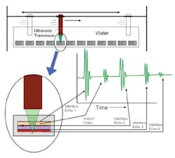
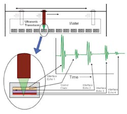
Figure 1 shows a typical setup. The ultrasonic technique for obtaining layer thickness is essentially a time-of-flight measurement of a pulse echo. The piezoelectric transducer focuses an ultrasonic pulse onto the tested material through a layer of water. The water provides a better coupling medium than air for transfer of the pulse energy to the part under test.
The transducer also acts as the receiver for the reflected echo pulses. At each material interface, there is a change in acoustic impedance that causes some of the energy in the pulse to be reflected back to the transducer. The echo arriving at the transducer generates a signal measured by the digitizer.
The timing of each echo allows for a measure of the thickness of each layer when you know the speed of sound within the sample. As the transducer is scanned over the part in raster fashion, a 3-D data set is assembled from which images are generated. The images can reveal and highlight flaws in the parts tested. In the case of semiconductor packages and circuit-board assemblies, they can reveal cracks, voids, disbonding, uneven lamination, and solder problems on ball grid array packages.
The requirement for efficient automated ultrasonic inspection of semiconductor packages is growing. Typically, entire trays of packaged chips are inspected at once by the scanning systems, and chips with flaws are easily detected and eliminated.
One such inspection system, made by a leading manufacturer of SAM systems in Japan, has a digital acquisition system based on the Acqiris AP101 and AP201 Peak Analyzer Cards.
These cards offer a system bandwidth of up to 1 GHz, sample rates up to
2 GS/s, and 1.2-�s dead time between acquisitions when segmented memory is used. This bandwidth, together with the proper transducer, results in a system that measures with a resolution down to 0.5 �m. Scanning speed and resolution are further improved using the segmented acquisition mode and sustained sequential recording.
Scanning speeds of the transducer over the part can reach 1,000 mm/s with up to 8,192 pixels per line. Data collection for each pixel is initiated by a trigger, usually generated coincident with each excitation of the transducer. Each pixel contains the data from the corresponding echo pulses.
The peak analyzer cards provide efficient data collection and transfer together with real-time peak detection and analysis capabilities. Regions of interest in the scanned part can be predefined with gates. The gates designate a region at a certain depth inside the semiconductor package, usually an interface layer, where flaws may occur.
Gates define a time region after the trigger where the system will analyze the signal and determine the echo peak amplitude and position. Gates are prepositioned by the user to align with regions of interest which correspond to each of the interface layers in the chip so that abnormalities may be found.
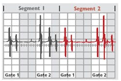
In Figure 2, several such gates per segment are used. Each segment in this case is 2,000 points, with each gate spanning nearly 600 points. The gates reduce the total number of samples that need to be processed. The gates are analogous to the gates previously used in the older analog peak-detection schemes.
Only the data of interest is analyzed and transferred. Unnecessary or superfluous data regions outside the gates are ignored.
Figure 2 shows a case where two gates per segment are selected for peak analysis. Up to 64 gates per segment may be defined. Each gate uniquely corresponds to a range of depth containing the interface of interest in the chip under test.
The peak determination is accomplished using an interpolation of the digitized data points near to the peak. This ensures that the true peak position and amplitude are found even if there is not a sample point directly on the actual peak.
The interpolated peak position and amplitude are calculated as 32-b values read out to the PC. The onboard signal processing enables higher data throughput rates, increasing the pixel density of the SAM image. This also means that SAM systems can measure larger areas with more detail while minimizing the total measurement time for each package.
Knowledge of the structure of the chip tested allows inspection tolerances to be set and abnormalities displayed on a false color scale, usually with red being the farthest out of tolerance. The system can be automated to eliminate particular chips from being placed in the end product. This ultimately can have significant cost-saving implications for every company in the manufacturing chain from chip to end product.
About the Authors
Phil Gregor is the U.S. product marketing manager at Acqiris. He joined the company in 1999, holds five U.S. patents, and belongs to the American Physical Society. Mr. Gregor graduated from the University of Massachusetts with a B.S. in physics. Acqiris, P.O. Box 2203, Monroe, NY 10950, 845-782-6544, e-mail: [email protected]
Greg Tate is the director of sales for the Acqiris Asia-Pacific Region. He received a B.S. in physics from the Royal Melbourne Institute of Technology, Australia. Acqiris Asia-Pacific, Suite 7, 407 Canterbury Rd., Surrey Hills 3127, Australia, 011 61 39888 4586, e-mail: [email protected]
FOR MORE INFORMATION
on acoustic tomography
www.rsleads.com/501ee-219
January 2005


