Along with the outstanding performance of today�s flash memory come the challenges of testing such devices.
The popularity of consumer products such as music players, cell phones, and digital cameras is fueling rapid growth for NAND flash memory, surpassing NOR revenues for the first time this year. Intense price competition in the consumer market translates into tight margins for the semiconductor industry, especially for subcontractors, making it ever more critical to achieve high utilization of capital equipment such as ATE. The industry is facing the triple challenge of responding to a fast-moving market, meeting new flash and technology test requirements, and lowering the cost of test for the consumer segment.
The rapid growth in NAND is credited by Gartner, a worldwide provider of research and analysis about the global information technology industry, as one of three major trends that helped push semiconductor revenues to a historic $235 billion in 2005. This is the first time that industry revenues have passed the $223 billion level reached in 2000. According to Gartner, the NAND flash demand is driven by strong sales gains for USB and flash card drives, digital audio players, and other portable devices.
NAND flash offers outstanding performance in data-dense applications that require low cost per bit and faster write times, and many of the year�s top product introductions feature large flash memory. For example, the new iPod nano includes up to 1 GB of NAND memory. Late last year, Motorola introduced a cell phone that stores 100 songs in NAND flash. Camera phones with 3 megapixels have hit the market, and 5- and 8-megapixel phones will be introduced later this year. All require large volumes of NAND flash.
Test Is an Understatement
It�s often said that virtually all memory devices are bad when they exit the fab and they are only made to work via the testing process. This is especially true of flash. As part of the test flow, internal voltage references are adjusted within the device, bad bits are mapped for repair or replacement (redundancy), and the cell infrastructure is programmed to optimize performance. These highly proprietary test methods, especially repair and redundancy implementation, require tight coupling between the device and the tester�s resources.
New features in NAND such as error correction coding (ECC) schemes add complexity to existing test challenges. In ECC devices, single or even multiple bad bits are allowed in the data content. These are corrected by the flash and memory controller and transparent to the user.
However, during test of ECC-enabled devices, the ATE must be able to distinguish between those errors that can and cannot be corrected by ECC. Bad bits must be differentiated as either ECC bits or must-repair faults during the test execution.
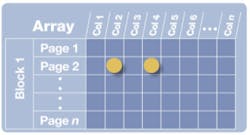
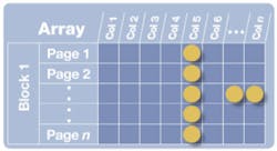
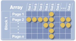
ATE must support both ECC bit logging as well as traditional bad element (row or column) and bad block/sector management schemes (Figure 1). The difficulty of this task is compounded by the variety of ECC methods in use. At the pattern�s end, the ATE must decide if the device has valid ECC failing bits (pass), bad but repairable redundant elements (pass), or maskable or replaceable whole blocks (pass), or just isn�t fit for your downloadable tunes (fail).
Figure 1. Typical Pass and Fail Combinations in NAND Flash
A Quart in a Pint Can
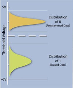
Multilevel cell (MLC) technology makes memory more dense and affordable by allowing each memory cell to store two bits of information, effectively doubling capacity (0 or 1 becomes 00, 01, 10, or 11). Today�s products overcome data reliability, performance, and flash management issues that were inherent in early MLC designs and, as a result, have gained many design wins, especially in mobile handsets.
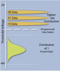
MLC flash particularly challenges the analog parameters of the device such as sense amplifier sensitivity and signal-to-noise ratios. Tighter distribution of voltages is required as multiple data threshold voltages (Vth) are squeezed into the cell�s gate programming range (Figure 2).
Figure 2. Threshold Voltage Distribution for MLC Flash
Wider deviations need more tuning or result in slower read operations. MLC also requires implementation of internal iterative or algorithmic processes to resolve the interpreted data result. These functions must be verified for each value and content of the multiple data bit stored in the memory.
Test and parameter coverage for MLC is more complex and longer than traditional, single data cell implementations and includes various stress, retention, and disturbance test suites. MLC implementation is expected to exacerbate weak bit/retention problems, further endorsing ECC implementations.
Stacks of Chips
While NAND flash is the hottest product in today�s memory market, many of today�s consumer applications require additional types of memory as well. For example, many high-end cell phones use memory architectures with NAND as the main data memory in combination with either NOR, DRAM, or sometimes both to execute the program code.
These different types of memory normally are stacked in multichip packages (MCPs) to create a single component. There also is a trend toward greater variation within a product family as each type of MCP becomes specialized to offer optimal performance within a specific application range.
The MCP also changes test dynamics since diverse individual chips can be quickly integrated onto MCPs, reducing the development and introduction time for new devices down to weeks or even days. ATE and interface suppliers must be responsive to these delivery demands and still meet the highest standards of quality.
Additional Demands on Test
Hybrid devices that have entered the market recently, such as Samsung�s OneNAND� and Spansion�s ORNAND�, provide additional complexities. These devices marry the feature set of NAND and NOR flash to combine the code execution capabilities of NOR with the data-storage capabilities of NAND in a single product. These devices require the same test coverage with their variant of protocol generation.
There still is further flash adaptation in Serial Peripheral Interface (SPI), a low pin-count implementation targeted for saving board space in commodity products. SPI relies on serial protocol and pin muxing to cram more information onto fewer pins.
While the internal array may seem traditional, SPI test must support serialization algorithms and include all the previous test coverage. Test vendors must provide solutions for these growing segments and new interface protocols.
In addition to standard protocols, most flash manufacturers use proprietary signaling interfaces and test methods. With design for test (DFT) implementations, built-in self-test (BIST), and logic vector support such as Verilog and STIL, the ATE needs to address many different interfaces to provide the flexibility needed to keep up with the fast-paced consumer market.
24/7 Only Part of the Test Answer
These trends pose major challenges for test manufacturing. The primary factors in the consumer markets that are driving NAND demand are cost and time to market. Integrated device manufacturers (IDMs) and subcontractors are under enormous pressure to ramp up volumes quickly to reap the maximum revenues for the short product cycles inherent in this market.
At the same time, to keep costs low, utilization and availability of capital equipment such as ATE become more critical than ever. In higher parallel test implementations, the unnavailability of the whole cell has a growing impact on utilization.
Changeovers, thermal stability, jam rates, and basic system reliability have a greater effect on overall system availability and a larger impact on cost of ownership. When a 512 simultaneous device test cell has a handling jam that halts production, the benefits of the massive parallelism quickly impact unit output.
And with massive parallelism also comes more difficulty in production line balancing. The capability to reasonably mix NAND, MCP, and traditional DRAM volumes gives many suppliers loading and utilization advantages over less flexible, targeted solutions.
Equipment uptime and utilization are critical components in a test cell�s overall cost of ownership. Cost of ownership in dollars/unit terms is calculated using the following general formula:
As a result, a percent gain in equipment uptime or utilization equates to an equivalent reduction in $/unit. A test cell that allows quick product changeovers, low mean time between failures (MTBF), and low mean time between assists (MTBA) or jam rates can significantly increase the equipment uptime and reduce the test cost. A test cell that is flexible to handle DRAM, NAND, or MCP testing can achieve maximum utilization and reduce the test cost as well.
Flash also challenges the test cell from a mechanical standpoint. Longer test times and huge volumes further increase the number of devices that need to be tested simultaneously.
The current installed base typically handles 256 to 512 devices per cell, and solutions for the next parallelism node already are beginning to appear. As the level of parallelism increases, tester pin-counts rise. This means that a 256-site ATE can easily require more than 30,000 pins.
In the interface, contacting these pins requires a high level of force that potentially creates both interconnect reliability problems for the cell and device ball damage. Neither is acceptable in today�s yield and cost-conscious consumer product manufacturing environment.
Staying Connected
As IDMs and subcontractors address these challenges, the traditional practice of considering each of the key elements of the test cell on a largely independent basis is rapidly becoming outmoded. The main components of the test cell include the ATE, package or wafer handler, and the two parts of the interface: the generic system interface and the device-specific adaptor that consists of a probe card or socket board.
As pin density increases, package types proliferate, and features increase flash testing challenges, it becomes critical to consider the entire test cell as a single unit. The performance of the entire cell rather than any of the components is the critical parameter required to reach the IDM�s or contractor�s goals.
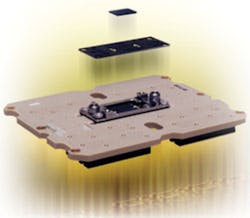
As increasing parallelism has pushed the density of the interface to unparalleled levels, the device interface board has become more critical than ever. For example, leading-edge memory socket boards have as many as 48 layers, making them some of the densest boards seen in any application.
The product yield depends on the integrity of the connection between the DUT and the socket board. The reliability and robustness of test depend on this last interconnect. Because of the high volume involved in memory applications, socket boards also have to fit economic models required for producing commodity components with ever-shortening life cycles.
ATE vendors address these challenges by performing detailed mechanical and electrical simulations of whole system constraints. These simulations make it possible to evaluate the performance of a multitude of design iterations in terms of the many components of the application, such as docking, contactor performance, and fatigue strength.
They also make it possible to evaluate new connector materials and geometries at a much faster pace than would be possible based on field experience alone. One of the most critical design issues is the trade-off between contact resistance, which is improved by increasing contact force, and contactor durability and ball damage, which are improved by reducing contact force.
With connectors approaching a pitch of 0.4 mm, contactor design becomes a gating limit. One of the most popular types of contactors is micro-pogo pins. These contactors consist of pins bored to make room for an internal spring that provides compliance needed for sufficient contact force without exceeding durability limits.
Another type is the micro-spring contactor in which the pin itself is made of a spring material. As an example of a new development, a recently developed socket offers less than 0.4-nH self-inductance, a >70% reduction from the previous model. The socket provides low transmission loss and suppresses reflection noise and power supply fluctuations. These new, low-impact sockets deliver low noise and higher bandwidths, often bringing substantial yield gains.
Package handling is another critical concern. Here the primary requirement is to move chips quickly from tray to socket and socket back to tray while avoiding damage to delicate devices. These DUTs can easily be damaged when plunging them into a socket and even by centrifugal force that is experienced in a fast, tight turn.
To minimize cycle time while avoiding g-force excursions, smart handler software is required to control the pick-and-place robots. Again, simulation optimizes this trade-off. As a general rule, new packages can withstand less g-force than the packages they replace so it is necessary to have a flexible, adaptable handling solution.
Summary
New features that are continually being added to flash memory ratchet up the testing challenge another notch. The extreme variety of feature sets offered by today�s flash and MCP devices and the certainty that tomorrow�s memory ICs will look much different than today�s put a premium on ATE flexibility and programmability.
Add to this mix an incredible volume ramp with global distributions of manufacturing. All together they represent a considerable challenge to semiconductor manufacturers and their ATE partners, which, from an ATE perspective, can be addressed largely with a test-cell approach and flash-specific features.
About the Author
Gary Fleeman is director of product engineering for Advantest America and an 18-year veteran of the company. Prior to joining Advantest, he held other positions in test and CMOS product engineering and strategic marketing and worked with the National Bureau of Standards. Advantest America, 3201 Scott Blvd., Santa Clara, CA 95054, 408-988-7700, e-mail: [email protected]
March 2006

