When asked, many engineers will say that the goal of a test plan for a PCB is full or 100% test coverage. When pressed further, they usually admit that 100% test coverage is virtually impossible to achieve. The real goal becomes optimum test coverage, which can be thought of as the maximum test coverage achievable given a set of restraining factors.
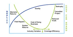
Cost is at the top of the list of restraining factors. Usually, an optimum test strategy boils down to achieving maximum test coverage at an acceptable cost level (Figure 1). Since no one technology can come close to full test coverage, optimizing a test plan for a particular PCB consists of assembling the right combination of methods and technologies so costs are minimized and coverage maximized.
Figure 1. Quality and Cost vs. Test Coverage
Why Optimize?
Striving for optimum test coverage is imperative to improve manufacturing yields and product quality, reduce product returns, and enhance the marketplace competitiveness of the product.
The prime reasons for a test strategy are to find defects, diagnose the cause of the faults, and repair them. Of course, fault data then must be used to constantly improve the processes that produced the PCB and the faults in the first place.
This feedback loop will drive down metrics like defects per million opportunities (DPMO). As an effective test plan causes DPMO to drop, yields on PCBs increase so that a higher percentage of the assembled boards moves from assembly to final system integration.
In many cases, achieving an optimized test plan may require adding capital investment in equipment. But this cost should be balanced against the cost-of-test for the life of the product. Amortizing test equipment costs over a product�s entire life cycle often reveals that the real return on investment can be high and the payback of its procurement cost very rapid.
Along with the cost of additional or incremental test capabilities, there are a number of considerations before a test plan can be finalized. For example, what are the capital assets such as test hardware and software that already are in place? Moreover, test equipment that requires a long development cycle might jeopardize the product�s production schedule.
In a manufacturing environment, beat rate, or the rate at which finished products must be produced, usually is of paramount importance. A critical factor in maintaining the necessary beat rate often is production line balancing.
In a balanced production line, a PCB will move steadily down the line, avoiding any prolonged stop at any one test station. If a specific defect can be detected at any of several test stations, the station with the shortest test time should be assigned to cover that defect to achieve a better balance.
Product-specific factors also must be considered. The unit volume over the projected life cycle of the product, for example, will affect acceptable yields. High-volume, low-cost assemblies can be more tolerant of poorer manufacturing yields while low-volume, high-cost PCBs require very high yields. Of course, the testability of a design, or how much testability was designed into the PCB, also will determine the test tactics that can be applied to the assembly.
Strength in Numbers
Because every test technology or methodology has a finite limit on the coverage it can provide, optimum test coverage usually is achieved through a combination of several technologies. The strengths and weaknesses that are unique to specific test methodologies steer each technology to a certain role in a PCB manufacturing environment. Broadly speaking, contemporary electronic test performs several distinct functions including process monitoring and structural test, electrical structural test, and functional test (Table 1).
Table 1. Matrix Listing Test Functions vs. Test Technologies/Methodologies
The most prevalent technologies that make up many test plans include automatic optical inspection (AOI), automatic X-ray inspection (AXI), manual visual inspection (MVI), in-circuit test (ICT), manufacturing defects analyzers (MDAs), flying probe test (FPT), boundary scan/JTAG test, and processor emulation. Several of these technologies, such as JTAG and ICT, or JTAG and processor emulation also can be combined in one test station, reducing the number of distinct stations and the complexity of the setup.
Functional test may require several technologies. System mock-ups, self-diagnosis, instrumentation, simulation, emulation, test executives, and others are methodologies frequently applied in functional test.
It is worth noting some of the strengths and weaknesses of the major test technologies since they often play an important role in achieving optimum test coverage.
JTAG/Boundary Scan
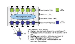
Boundary scan or JTAG, named for the Joint Test Action Group that developed the original specification, is a relatively inexpensive technology that offers very high structural test coverage around the JTAG-enabled devices on a PCB. Since it functions by stimulating and monitoring nets and connections on the PCB through chip-level registers, boundary scan is one of the few truly nonintrusive test technologies (Figure 2). It requires no costly fixtures or on-board test points, and it places no added stress on the PCB.
Figure 2. Boundary Scan Cells in a Chip
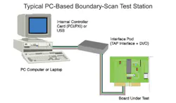
With the right JTAG system, test development can be highly automated, and diagnostics can quickly isolate faults. The JTAG infrastructure on a PCB also can be used for on-board programming of flash memory and configuring programmable logic devices and field programmable gate arrays (FPGAs) (Figure 3).
Figure 3. Typical PC-Based Boundary Scan Test Station
The boundary scan standard, IEEE 1149.1, has been adopted as the basis for a number of related test and programming standards. There also are some standards still being developed: IEEE 1149.6 for testing high-speed
AC-coupled buses; IEEE 1532 for concurrent programming of multiple devices on-board; IEEE P1687, a preliminary standard for embedded test instrumentation; Intel IBIST for embedded self-test of high-speed buses; JEDEC�s STAPL standard for on-board programming;
the System JTAG initiative; and PICMG�s MicroTCA standard, which includes JTAG as an optional test method.
The effectiveness of boundary scan test can be limited when there are few JTAG devices on the PCB. Its role in analog test also is limited.
Manufacturing Defects Analyzers
Developed in the 1970s, MDAs require a test fixture with spring probes specific to each PCB. The probes make contact with test pads on the PCB, placing added stress on the circuit board.
An MDA is relatively inexpensive, and test development has been automated. An MDA uses a low-voltage stimulus to detect shorts and component values. Since an MDA cannot power up digital devices on a PCB, it can detect some, but not all, opens.
In-Circuit Test
ICT systems are capable of high structural test coverage on nets and pins where physical access such as test pads can be contacted by spring probes. Beyond the initial expense of the ICT system itself, fixtures and their maintenance can be expensive.
ICT can test for shorts and opens as well as make analog measurements and perform digital tests to find opens and verify whether the correct digital device has been placed on the board. Test development is automated and diagnostics thorough. ICT also can program flash memory and configure logic devices and FPGAs on-board.
Flying Probe Test
In contrast to the many physical probes in an ICT fixture, FPT systems usually have four probes which are moved to access points or test pads on the PCB. Because the test heads must be moved, a complex FPT test can take considerable time to complete. This usually rules out the use of FPT in high-volume manufacturing applications.
Since no fixture is required and test development is automated, FPT is relatively inexpensive. It often is used for testing prototype PCBs. FPT offers good coverage and diagnostics for shorts and analog measurements, but its coverage of opens is limited. It places little stress on the circuit board.
Automated Optical Inspection
AOI has advantages because it is nonintrusive, does not require a fixture, and does not place additional stress on the circuit board. By using visible light and laser reflections, AOI can detect the presence and type of chips, their alignment, and orientation.
It also can identify process anomalies such as solder cracks that could go undetected with electrical testing. Although the condition of some solder joints can be studied, those that are under chips in ball grid array (BGA) packages, other types of chip-scale packaging (CSP), and heat sinks cannot be seen by an AOI system. Of course, electronic defects will not be detected at all, and consistent test repeatability can be a concern.
Automated X-Ray Inspection
AXI captures layers of X-ray scans so it can inspect inside and under any
semiconductor device or heat sink. It can check solder joints for voids and cracks.
Like AOI, AXI is noninvasive, fixtureless, and stress-free on circuit boards. Because of the complexity of the technology involved, it is relatively expensive, and inspection times can be excessive. As a result, AXI sometimes is deployed for off-line analysis of failed PCBs instead of for in-line test. As with AOI, test repeatability also can be a concern.
Applying the Test Technologies
Often when investments are made in test technologies and personnel training, isolated silos may begin to grow up around the various test technologies and the people who operate them. For example, those responsible for AOI might not confer with the ICT people as often as they should. Likewise, engineers working with JTAG test stations might have little contact with the FPT experts.
This is unfortunate because only through collaborative and coordinated efforts can an optimum test plan be achieved. The test-silo approach could lead to unnecessary and costly redundancies among the test technologies. Or, overall test coverage might fall short of what could be cost-effectively achieved. Optimum test plans emerge from collaboration and teamwork.
In addition, common misconceptions sometimes get in the way of achieving an optimized test plan. For example, some test engineers may have inaccurately pigeonholed JTAG as an inexpensive way of testing prototypes in design debug but redundant to ICT in manufacturing test. In actuality, boundary scan and ICT can complement one another quite effectively.
On densely populated PCBs with several BGAs and other high-speed devices, space on circuit boards for test pads may be hard to come by. These types of devices are prime candidates for JTAG test since they usually have the JTAG infrastructure built into them. The boundary scan tests developed during design could be applied to ICT in production while traditional ICT is applied to other sections of the PCB that feature analog components.
Similar to the relationship between JTAG and ICT, the give-and-take between structural and functional test also could bring down costs while increasing coverage. In many cases, structural test, which verifies the quality of an assembly process by testing physical elements and their interconnections, can more effectively diagnose the root causes of faults than can functional test, which verifies that the PCB, subsystem, or system performs as intended.
Moreover, structural test technologies like JTAG often are less expensive than the rack-and-stack setups, instrumentation, and other technologies that typically are deployed in functional test. Other advantages of structural test over functional include faster execution times, easier development techniques with a high degree of automation, and the capability to quantify and compare expected coverage metrics.
Shifting some of the responsibility for test coverage from functional to structural test may make sense, but structural techniques also have their limits. For example, the effectiveness of structural test technologies often hinges on the design-for-test features designed into the PCB.
Functional test techniques also can detect certain structural faults. In the end, the balance between functional and structural test usually depends upon the design of the PCB, the test processes in place, and the overall test strategy for the PCB.
Quantifying Test Coverage
Developing a high level of confidence in a test plan made up of multiple technologies as well as several different types of test like structural and functional can be a daunting task. The variables are many and interrelated. And a person�s role in the organization can affect how and why they quantify test coverage.
Program managers typically want a single number, percentage, or ratio that will tell them whether the product is ready to move into production and what the manufacturing yields will be. Developers of test strategies want to look at a matrix that shows which technologies deliver the coverage expected and which ones still need more work. And the development engineer wants to know when he can stop developing tests. He derives this information from a ratio of coverage attained vs. total planned coverage.
Several standards for modeling test coverage have been proposed by companies as a way for the industry to share a common vocabulary and facilitate the exchange of coverage data among test systems and technologies.
In the realm of structural test, Agilent Technologies has outlined the PCOLA/SOQ method. Each letter represents a characteristic of a device or the PCB that must be verified. The PCOLA/SOQ acronym stands for Presence (Is the device present?), Correct (Is it the correct device?), Orientation (Is the device oriented correctly?), Live (Is it functional?), Alignment (Is the device aligned properly?), Short (Is there a short in an interconnect?), Open (Is there an open in an interconnect?), and Quality (What is the quality of the solder joint?).
Another structural test coverage methodology has been described by Aster Technologies in France. Aster�s PPVS method focuses on Presence, Polarity, Value, and Solder. Philips Research in the Netherlands has proposed the MPS method for Material, Placement, and Solder.
Several other standards add functional test criteria to the structural factors. For example, the International Electronics Manufacturing Initiative (iNEMI) has expanded PCOLA/SOQ to PCOLA/SOQ/FAIM with the addition of functional characteristics Feature, At-Speed, In-Parallel, and Measurement. Philips has expanded MPS to DMPSF, which includes Design and Function.
This movement toward a standard way of measuring and talking about test coverage is beneficial to test equipment suppliers, software vendors, and electronics manufacturers. But users of such standards would benefit the most if the industry would settle on one methodology.
With one way of measuring test coverage, one reporting format could be shared so that information from different types of test technologies would be combined into one easy-to-understand report. It also would improve the reliability of manufacturing yield predictions since the same test coverage metrics from the various technologies could contribute to an overall fault probability projection for the PCB.
Getting More for Less
Given the fact that 100% test coverage is virtually impossible to achieve, the optimum plan for a particular PCB revolves around a set of trade-offs. But within this constellation of trade-offs, the defining relationship is that between test coverage and cost.
Investing in technologies or new processes which increase test coverage only makes financial sense to a certain point, after which the return on each incremental dollar invested diminishes and can eventually become negative or just another cost. The challenge for test strategists is to devise plans incorporating less costly test technologies that offer the same or better coverage�certainly a formidable challenge in anyone�s book.
About the Author
Arden Bjerkeli is director of customer applications support at ASSET InterTech. Previously, Mr. Bjerkeli was at Compaq Computer where he was responsible for the test strategy for desktop computers and server products. ASSET InterTech, 2201 N. Central Expressway, Suite 105, Richardson, TX 75080, 214-540-2964, e-mail: abjerkeli
asset-intertech.com
FOR MORE INFORMATION
on boundary scan
www.rsleads.com/709ee-181
September 2007
About the Author
Voice Your Opinion!
To join the conversation, and become an exclusive member of Electronic Design, create an account today!

Leaders relevant to this article:


