Designing a load board or circuit board for IC testing sounds like a routine task that involves a few basic requirements and some common-sense approaches. But it’s not always that simple. With new technologies and increasingly complex design requirements, there now are more issues than ever to consider in optimizing a load board.
Some factors, like substrate material selection, are fundamental. Others differ with specific designs, including board layout; component placement; the number, placement, and size of vias; load board grounding; and pad sizes. These factors all help minimize crosstalk. Many times, modeling ties all of these components together to determine if the electrical performance will be met before the board is fabricated.
Substrate Material Selection
Choosing the correct substrate material is critical for good load board design. The most important individual electrical parameters are a low dielectric constant and a low dissipation factor or loss tangent. Also, if the system is going to be measured across a wide bandwidth, consistent performance across a broad frequency range is crucial for accurate signal reproduction.
Be sure to consider the proper substrate thickness. This is important in determining the geometry of the rest of the load board because the distances from the ground plane or planes will affect the impedance of the signal line. Standard high-frequency materials are only stocked in 5-, 8-, 10-, 15-, 20-, 32-, and 64-mil thicknesses. Usually, 4 mils is the thinnest available substrate material.
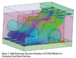
Sharp corners on the trace stub have higher E-field concentrations so it is best to radius edges and reduce the stub lengths. The E-fields on the left side of the model are reduced in magnitude primarily due to a cutout in the housing above the traces. The top right side of the model (the green box) is the DUT.
Many load boards are designed to test parts on the production floor in a removable contactor. Often, the load board/contactor system is compared with the process of directly soldering parts to boards to calibrate out extra losses.
Whenever a test contactor is used, it will increase the amount of ground inductance because the device will come to rest some distance above the load board. For that reason, it is vital to design the load board with lower ground inductance than is needed to make sure you still can test parts to specifications in production and that extra parameters or losses due to the contactor don’t affect yields.
In cases where the system is repeatable, these extra losses can be calibrated out. If the gain of an amplifier is measured, the amount of lost gain is affected by how low the ground inductance is in the test contactor.
Board Layout
Typically, when laying out a load board, it is better not to introduce any stubs that will act as antennas and degrade the performance. This often occurs when the board is laid out for two different technologies or when devices are soldered to the board in addition to testing with a contactor.
Solder mask should be removed from the area under the contactor to make sure it sits flat and the devices are presented in a coplanar fashion. This provides the added benefit of increased contact and contactor life. If it is necessary to run parallel traces, it’s best to route signals in differential format ground-signal-signal-ground (GSSG) to reduce the susceptibility to noise.
Using screw-on connectors for high-frequency RF signals also can improve performance. The best performance comes when the connectors are in line rather than vertical through the board. Any posts on the connectors, both grounds and signals, should be flush to prevent any unwanted stubs and degraded performance.
Component Placement
Ideally, decoupling components are located right behind the contactor contacts they are meant to decouple. This is particularly important at high frequencies. If this is not done, the decoupling can actually exacerbate the situation because the length of circuit trace or wire between the target contact and its decoupler acts as an antenna. This allows noise to enter or exit the circuit. This same length of circuit trace or wire can form a resonant circuit with the decoupling components and cause sporadic oscillations.
Since it is desirable to have the decoupling components located right behind the contact they are to decouple, the frame of the contactor may need to be modified for the decoupling component placement. Using a universal arrangement allows a specific contactor to accommodate several different types of packaged devices.
The placement of tuning elements closely follows the criteria outlined for the placement of decoupling components. Elements comprising phase-locked loops (PLLs) are particularly sensitive to noise.
A common practice with high-speed digital devices is to embed all the elements of the clock recovery PLL internal to the chip itself. However, the capacitors that set the corner of the low-pass filter of the loop are external to the device. They are placed on the load board.
For optimum performance, these capacitors must be located directly adjacent to the terminals to which they belong. Since they are susceptible to noise pickup, they must be shielded using a guard-ring trace around these capacitors on the PCB or load board.
Vias
The number, placement, and size of vias are important considerations in a successful load board design because vias route signals between layers and act as vertical shields between traces. A via hole is a location in a PCB used for either mounting a through-hole component or routing traces between layers. Since vias typically carry electrical signals or currents, they are plated for continuity. Vias can serve as a path to ground from traces on one layer of a PCB to the ground plane.
In most instances, vias are the most direct path to ground. In high-speed digital and RF designs, ground paths must be short and direct to avoid introducing extraneous noise into the circuitry. In many cases, boards have an insufficient number of vias to adequately test a part without impacting its performance, especially at elevated frequencies or at gains above 30 dB.
There are two basic types of vias: standard and micro. The design choice depends on factors such as frequency of operation, trace density, parasitics, and economics and includes a basic trade-off between density and cost.
If a via is used for mounting a component, then it must be large enough to accommodate the lead of the component with adequate allowance for plating buildup and solder. Small via holes require small drill bits, and laser systems are used for vias that are less than 4 mils in diameter.
The drill bits used for these small holes are more prone to breaking than big drill bits, adding to the fabrication costs of the load board. Also, small bits wander off center, a characteristic that increases production costs since boards must be drilled in small batches.
Microvias, which are made by photoimaging, laser ablation, or plasma etching, generally are used in very high trace density designs. Microvias can be 2 mils or smaller. Accordingly, the density of pads can increase fourfold. Microvias also can be placed directly in pads, creating even more space savings over standard vias.
Via hole diameter depends on the thickness of the PCB or load board. Standards have been established and documented for this purpose including MIL-STD-275E, which lists the acceptable hole diameter for a standard via as T/4 where T is the board thickness.
The more vias between the top layer ground traces and the ground plane, the lower the effective ground inductance and the better performance. Typically, the lower the loss tangent, the less loss occurs in the substrate.
A low dielectric constant and a hard substrate are important for high-frequency testing in production. The RF or sensitive traces usually are on the perimeter of the package so it is best to route them on the top layer of the substrate to reduce losses. These will be either microstrip line structures or coplanar waveguide structures.
Typically, the impedance of the DUT will be 50 ?, matching the test equipment. To get the largest bandwidth, the contactor and load board also should be designed for 50 ? to prevent mismatch errors. If matching is done on the load board for a particular frequency of test with lumped elements, the performance generally will be worse if you use a different contactor technology.
Load Board Grounding
Increasing the number of paths to ground also reduces the ground inductance and tends to increase the bandwidth of the system. Positioning vias periodically about 1/20 wavelength apart between the ground pad or trace and the ground plane effectively places a shield box around the signal trace. The higher the frequency of the signal trace, the closer the vias need to be to control crosstalk.
Isolation and crosstalk can be mitigated by simply placing a ground trace between two signals. The improvement can be more than 20 dB at lower frequencies and at least 10 dB at higher frequencies.
Guidelines for load board grounding optimization include the following:
• The length and area of the ground path are very important to match the DUT.
• Ground inductance should be minimized to optimize higher frequency performance.
• Ground resistance should be low to minimize power supply voltage drop.
• Grounding via fences controls crosstalk between signals by creating a wall between signal lines.
Pad Size and Shape
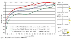
Both the pad size and shape affect the reflections and radiations and consequently the bandwidth. As a simple example, three pad layouts were chosen to calculate the effects. In Figure 3, Layout B is the largest pad with square corners, Layout A is slightly smaller, and Layout C is smaller yet and with rounded corners. Using the 15-dB point to define the bandwidth from the return loss yields 4, 7, and 24 GHz, respectively, for Layouts B, A, and C.
This suggests some rules for board layout around the contactor: pick trace widths that are 50 ? and that support the contact and land on pads that don’t create stub effects. The return loss degrades rapidly the larger the stub becomes beyond the contact and load board interface. Large board mismatches and stubs create mismatch losses that will affect the insertion loss of the system, creating changes in measured gains of amplifiers or other active components.
If insertion loss bandwidth is specified as the 1-dB loss point, the pad that is longer than needed can create a large stub, decreasing the 1-dB bandwidth by almost three times compared with an optimum pad with a very small stub. For this modeled system, the bandwidth is 37 GHz for the optimum pad layout and only 14+ GHz for the pad that would allow soldering the device to the load board. The trace width doesn’t affect the response much as long as the width is designed to be close to 50 ?.
Minimizing Crosstalk
When routing high-frequency traces on the load board, it is vital to note that right angles tend to radiate more energy because signals propagate in straight lines. Changes in line width result in changes in impedance and cause reflections. Placing a ground trace between high-frequency lines creates a barrier so signals remain confined.
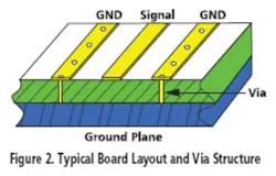
Placing a via fence like the one shown in Figure 2 further prevents unwanted signals from appearing on adjacent traces. Clock lines have higher frequencies, and good clock edges require the 3rd and 5th harmonics. Decoupling components should be located close to the device. For best contactor performance, match the trace impedance to the device.
As traces move from the edge of the board to a device, they tend to get closer together, reducing their impedance. One effective method for maintaining impedance of the traces is to narrow traces slightly as they get closer to a contactor and the DUT.
In summary, to minimize crosstalk:
• Isolate high-frequency traces using ground lines.
• Isolate high-frequency traces using via fences.
• Move clock traces away from other signal lines.
• Route sensitive lines first: high frequency, clock lines.
• Reduce parallel trace runs. The longer traces run side by side, the more crosstalk.
• If parallel traces cannot be eliminated, route the signal as a differential pair.
Electrical Performance Model
Modeling typically is used in the design phase to determine the system performance and usually includes all the system parts: load board, contactor, and device. Modeling helps predict performance. If done properly, it often results in the correct design of a high-performance load board on the first try.
To optimize performance, modeling matching networks generally is used to improve the test results, especially if only one frequency is of interest or a narrow bandwidth of frequencies is important. If the frequency is changed or contactor performance changes, the match will not work as well after the change and often can degrade the performance. Obviously, it is important that all the components of the system have the required bandwidth needed to test the DUT. Matching to optimize performance usually is successful at one or a limited number of frequencies.
In conclusion, many factors play into designing a load board that will result in an effective test of the DUT. Neglecting just one of the factors, such as substrate thickness and material selection, via placement, signal routing, or grounding, can result in redesigning the load board. Modeling, if done correctly, will tie everything together. Accurate models that predict performance will identify issues early and often result in a successful first design.
A Few Basic Tricks of the Trade
About the Author
Jeff Sherry is a senior RF/high-speed digital R&D engineer at Johnstech International. He has 25 years of semiconductor industry experience in designing and modeling microwave circuits up to 100 GHz. A licensed professional engineer, Mr. Sherry received a B.S.E.E. and an M.S.E.E. from the University of Minnesota and an advanced technology degree through Honeywell. Johnstech, 1210 New Brighton Blvd., Minneapolis, MN 55413, 612-378-2020, e-mail: [email protected]
About the Author
Voice Your Opinion!
To join the conversation, and become an exclusive member of Electronic Design, create an account today!

Leaders relevant to this article:


