A finite element analysis of copper pillar bump probing
In 2001, IBM patented a method of using a double bump material structure to make a reliable joint between a chip and its package for bump pitch below 150 µm.1 This invention improved the existing flip chip method in the electronic package industry, also developed by IBM circa1964, commonly called C4 (controlled collapse chip connection) technology. The C4 method is based purely on the reflow of solder bumps. During reflow, the solder bumps collapse without maintaining the initial height, sometimes creating shorts between adjacent bumps if the distance between them is too tight.
A new package connection process, known as copper pillar (CuP) technology, is a paramount component of flip chip interconnection for 28-nm wafer technology and 3D IC integration. The original concept of CuP described a bump structure as a copper post (pillar) with a solder cap on the top. The copper post is in contact with the chip structure and the solder cap with the package. Using the different level of melting temperature between two materials was an innovative idea of the IBM patent. Over the years, CuP technology had many improvements with more than 120 U.S. patents related to this process.
The development of complex and advanced test probe cards requires a judicious combination of experimentation and modeling. The probe cards with 15,000 or more probes used for multi-DUT parallel tests are economical solutions that reduce the wafer test cost. The key to repeatable and high probe card performance is the probe design, which can minimize the damage of the very thin solder-cap layer and reduce the stresses in the bump structure during the wafer test, avoiding cracks and delamination of chip layers underneath the pillars.2,3
Finite element model of CuP bump
Today’s finite element analysis (FEA) has become sufficiently mature to develop reliable insights into the mechanical integrity of composite structures such as CuP bumps and chips. The important advantage of FEM is the calculation of deflection, stress, and strain of the entire, very compound design. The graphical interpretation of the FE results allows a better understanding of the bump stress distribution as well as providing a better engineering assessment of the critical stresses for each material layer.4
The present study utilized the commercial finite element software ANSYS 15.0 to obtain the comprehensive results and introduce the bump geometry and material properties influencing the model response.
The study presents a model of a probe tip in contact against a hemispherical CuP bump and chip structure. The probe tip is flat and rigid and 50 µm in diameter. The CuP bump has a cylindrical shape with a hemispherical solder cap. The copper post diameter is 50 µm. The overall height of the CuP is 75 µm, including the copper post’s 50-µm height and the solder cap layer’s 25-µm thickness.
Both 2D and 3D ANSYS models have been developed for evaluation. To improve the efficiency of calculation, axisymmetric models were used.
The 2D model used PLANE183 (axisymmetric), SURF153, CONTA172, and TARGE169 parameters. The model meshing created 2,924 elements. The SOLID186, CONTA174, TARGE170 parameters were used for the 3D model, which had 20,875 mesh elements.
The fine model meshing is applied near the top of the solder cap. To ensure the accuracy of the analytical results and conduct convergence analysis, a mesh refinement was implemented. Primarily, the 2D model has been used to reduce the calculation time. The 3D model was used for graphical illustration of stresses and strains of the studied structure.
The model’s material properties, except the solder cap, were considered to be linear-elastic, homogeneous, and isotropic. The solder cap is considered as a nonlinear, bilinear-elastic plastic material. A bilinear-elastic plastic material model accounts for strain hardening of the material beyond its yield point. The maximum stress of each material layer has been determined by the von Mises stress criterion.
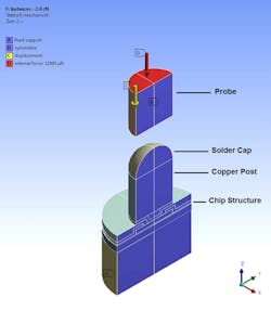
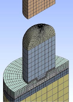
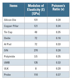
Figure 1 shows the sectional 3D model with boundary constraints. The model nodes at the base of the silicon are fixed in all directions. The defined forces were applied vertically on the probe. Deformable-deformable contact and the augmented Lagrange method with an initial friction coefficient of 0.2 were used in the model setup. Figure 2 is showing a close-up of the model meshing. The corresponding material properties such as modulus of elasticity and Poisson’s ratio are listed in Table 1.
Click image to enlarge
Results and discussion
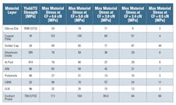
The CuP bump structure is composed of several material layers, each with a distinct yield strength. The maximum stresses in each layer are calculated using a range of forces applied on the model from 0.5 cN to 6.6 cN. Table 2 shows the yield strength and the FE calculated maximum stresses for each.
To verify the FE calculations, two probe cards were built with specific force values: 6.6 cN and 2.4 cN. The production wafer tests were conducted to define the solder cap deformation size and confirm that there were no cracks in the layers beneath. Extrinsic parameters, such as the strain rate and testing temperature and intrinsic parameters like the microstructure, were kept constant.
The FE model with applied force of 6.6 cN calculated the total deformation size of the solder cap as 26.6 µm in diameter and deformation depth as 4.53 µm. In tribology, deformation depth is called interference. After wafer sorting, the measured bump deformation diameter was 26 µm. Based on the manufacturing specification and guidelines, a deformation this size was too large and failed an optical test.
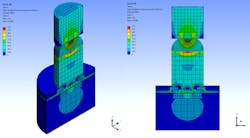
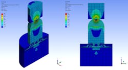
Figure 3 depicts a color-graded stress distribution map of the described 3D model. It is important to notice the high stresses in the copper post which might induce delamination between the solder cap and the CuP. The extent of the stress is quite large, reaching down to the silicon and causing high stresses in all layers. The maximum stresses in the solder cap, CuP, and UBM are beyond the yield strength point. Even if low plastic deformation of the solder cap is harmless, the high stresses in the layers underneath the post are dangerous and could lead to failure. Some production reports have described these types of failures when probe cards were used with probes having high spring forces.
Click image to enlarge
Figure 4 shows the stress distribution in the model with applied force of 2.4 cN. The calculated deformation diameter of the solder cap was 18.2 µm with1.74 µm of interference. The production wafer measurements revealed deformation 18 µm in diameter. The manufacturing metrology has accepted this size of bump deformation. The wafer post-process development has shown that there were no cracks or delamination in any intermetallic layers. When using the lower spring force, the maximum stresses in the CuP are shallow and below the yield points.
Click image to enlarge
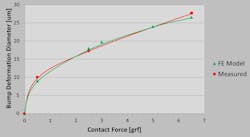
Figure 5 compares the FE model and production wafer measurements of bump deformation diameter as a function of contact force. The green curve depicts the model calculations and the red curve production measurements. The results of simulation are correlated quite well with wafer post-process readings, though they are slightly different in magnitude.
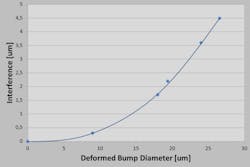
Figure 6 illustrates the FE model calculated interference as a function of deformed bump diameter. Initially, at small interference, the solder cap is deformed rapidly with a high strain rate. Eventually, as interference increases above 0.4 µm, the bump strain rate swiftly begins to decrease.
Conclusion
This work presents a finite element model of a CuP bump in contact with the flat rigid surface of a probe tip. The FE simulation calculations were compared with production wafer test results. The subsequent plots indicated that the FE modeling correlates well with the wafer floor test data. It was concluded that this FE model is reasonably accurate as an assessment tool for engineering probe card analysis.
It helps to understand the configuration of stresses and strains in the CuP bump and chip structure. This study reveals that an appropriate analysis of a real probe card combined with modeling can improve the design and reduce wafer test failures. Furthermore, the described approach can be a good reference and guide for future design analysis of fine-pitch interconnections, CuPs, and micro-bumps.
References
- Saitoh, K., et al, “Bump structure, bump forming method and package connecting body,” IBM U.S. Patent 6229220, May 2001.
- Wittig, A., et al, “Probing Study of Fine-pitch Copper Pillars,” SW Test Workshop, San Diego, CA, 2013.
- Grimm, K., et al, “3D TSV Cu Pillar Challenges & Experience,” SW Test Workshop, San Diego, CA, 2014.
- Dabrowiecki, K., and Behr, J., “Experience in applying Finite Element Analysis for Advanced Probe Card Design and Study,” SW Test Workshop, San Diego, CA, 2015.
Acknowledgment
The finite element models were prepared at Feinmetall by Jörg Behr, and the design and assembly of test probe cards were done by Lisa Schwarz, Uli Gauss, and Micha Frerichs.
Author’s note
This article is based on a paper, “Experience in Applying Finite Element Analysis for Advanced Probe Card Design and Study,” presented at the 2015 SW Test Workshop in San Diego, CA.
About the author
Krzysztof Dabrowiecki is the product manager at Feinmetall, Germany. He has been working in the probe card industry for 20 years as a part of the R&D and engineering teams for several products such as DuraProbe, VertaProbe, VertProbe, and MEMSProbe. Mr. Dabrowiecki earned an MSc in mechanical engineering from Gdansk University of Technology, is a member of ASME and IEEE, has authored numerous presentations in the areas of wafer test solutions, and holds four U.S. patents related to wafer sort and package test solutions.
About the Author
Voice Your Opinion!
To join the conversation, and become an exclusive member of Electronic Design, create an account today!

Leaders relevant to this article:
