“Auxless” GaN Flyback Converters Tackle AC-DC Adapter Design Challenges
Members can download this article in PDF format.
The impetus to reduce power demands of just about every device out there is the mantra of today’s power ecosystem. Manufacturers are under tremendous pressure, for both existing and emerging devices, to reduce footprint, power demands, cost, and complexity.
But this pressure is ramping up in the low-power segment because so many devices are going portable. For platforms such as USB—the focus of this discussion—wearables, sensors, and other small form-factor designs, power efficiency, footprint, and complexity are what receive top billing.
Sponsored Resources
- Innovative technology to simplify your designs
- Shorten time to market with self-biasing operation
- High efficiency across your entire load range
One groundbreaking approach is to update mature designs with new and innovative approaches. For this discussion, the flyback converter used in portable AC-DC supplies is simplified with a new semiconductor material—a gallium-nitride (GaN) high-electron-mobility transistor (HEMT).
While GaN has been around since the 1990s, its widespread use did not come on the scene until a few years ago because of cost. Its adoption was hastened by the increasing demand for smaller, higher-power adapters, which has helped it scale economically to within many device budgets.
Gallium nitride offers a laundry list of advantages, including high electron mobility and saturation velocity, a wide bandgap, excellent thermal conductivity, and high power density. Its significant improvement over silicon is its 3.4 eV bandgap, compared to silicon’s 1.12 eV bandgap. This wider bandgap can sustain higher voltages and higher temperatures. These two characteristics are the gateway to smaller, more efficient circuit designs.
Flyback Converter Design Thoughts
With GaN, designing flyback circuits becomes simpler, primarily because there’s no need for the auxiliary winding—and because GaN replaces the silicon substrate. This advance has led to “auxless” flyback design.
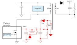
Auxiliary windings are a simple and inexpensive way to perform necessary functions, such as bias, common-mode noise isolation, and sensing (Fig. 1). However, they add bulk and cost to the power supply.
To improve the performance as well as reduce the cost and footprint, TI recently developed the UCG28862 self-biasing flyback network with integrated GaN. This device is the next generation of flyback converter biasing for low power (up to 65 W) supplies.
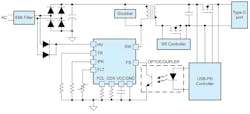
For this type of power supply, GaN-based, auxiliary-less primary-side regulation eliminates the need for the auxiliary winding and its related components. It also takes over sensing and isolation requirements. Thus, designs are simplified, costs shrink, and efficiency is improved (Fig. 2).
Another Tool for the Engineer
The TI auxless flyback converter is a great new tool for designers of the portable AC-DC power-supply market. The demands of some of the emerging and evolving devices require a much tighter, higher power, and smaller footprint regulated supply than transformer-based designs.
Such is particularly true for supplies that provide variable outputs. The auxless converter is also an ideal solution for the next generations of AC-DC USB Type-C devices. Moreover, it’s well-suited for programmable logic controller (PLC) applications.
Digging Deeper on the Auxless Converter
The obvious advantages of the converter have already been discussed. However, let’s drill down a bit more on some of these. Just knowing that something is simpler to design, or costs less, often isn’t sufficient for the engineer to determine if it’s suitable for purpose. If the simplified design can’t meet specific parameters, then it’s of no use.
Most engineers are familiar with conventional converter design. Typical design uses transformers and optocouplers to achieve galvanic isolation at the power and feedback stages, respectively. Although optocouplers provide a convenient way to measure output voltage error, they’re highly nonlinear, and its transfer function depends on both temperature and time.
There’s a relationship between the upper temperature limit of the optocoupler and its operating conditions, limiting the converter’s operating environment. To address this, the overall size of the total solution typically must be increased, which oftentimes isn’t an option.
There’s also lifetime degradation of the current transfer ratio (CTR) of the optocoupler. And if that weren’t enough, because of the extra pole introduced by the optocoupler, transient response is limited.
One can see why an alternative solution is desired. Losing the optocoupler immediately widens the application base for the converter.
The auxless transformer design enables a simpler magnetic structure with lower leakage inductance and opens up more choices in terms of low-cost, smaller footprint, and off-the-shelf components.
Obviously, however, the functions provided by auxiliary winding are lost with its elimination, yet they’re still required. How they’re recovered in the auxless designs is by examining the primary-side switch-node voltage. A lot of information can be gleaned by sensing this value.
The switch-node voltage is a scaled-down version of the output of the primary winding. The approach is to sample this voltage and apply signal discrimination techniques when the output diode is at the end of its conduction mode. Data gleaned by this method can manage several other parameters that were formerly provided by the secondary winding.
Subsequently, with a knee-position detection method of the switch-node voltage, and a sample-and-hold circuit, it’s possible to achieve highly accurate output regulation over wide load, line, and temperature ranges. In addition to control of other values like flyback settings, I/O voltages, load changes, and line changes are managed by the GaN-based IC. Bias and EMI management is also handled by the IC.
Conclusion
Gallium nitride presents advantages in a variety of KPIs. Depending on the topology, GaN-based platforms can be used to obtain higher efficiency or increase the power density, thus reducing the size of the application. Overall, a flyback with a GaN switch offers higher efficiency across all metrics, versus a similar solution on silicon.
To find out if the TI auxless converter is a good fit for your application, TI has the UCG28826EVM-093 evaluation module available.
Sponsored Resources


