Let’s say you’re into carpentry, and you’re building an heirloom-quality desk as a gift. You’re definitely going to “measure twice, cut once” at every step, to ensure that every piece of wood joins to the others precisely as designed (Fig. 1). It might take you some time to finish the job, but the resulting piece will be something that will last and be admired for years, if not centuries.
1. The required level of accuracy and precision are often determined by form and function.
But what if you’re just building a frame to hold your outside firewood supply? You probably don’t care if one end sticks out a bit or is slightly uneven, because it won’t significantly affect the functionality or the aesthetics of the frame. You’re waiving the precision of your measurements, at least within some tolerance range, so that you can get the job done faster.
This same tenet holds true in integrated-circuit (IC) design as well. Layout engineers responsible for debugging and correcting design-rule-checking (DRC) errors know that not every error result is equal. Some errors must be corrected to ensure the design is manufacturable and will perform as intended for the intended life of the product. Others are insignificant in that context, and not worth spending valuable time on debugging. But what to do with that knowledge?
That’s where design rule waivers come in. The concept of waiving, or ignoring, selected DRC results has been around for decades. There are many reasons for waivers:
- It may be impossible to code a rule that accurately catches all of the intended errors without also flagging some false errors.
- An error may be real, but upon review, it is determined that its impact to the chip yield and functionality is so minimal that time is wasted trying to fix it.
- In the rarest of cases, an error result may create a significant yield impact, but for chips with high profit margins and high demands, the design company may be willing to tolerate that yield hit to meet market pressures.
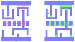
Historically, error waiving was done on a chip-by-chip basis. Before agreeing to manufacture a design, the foundry or fab would review known errors one by one to determine the significance of their impacts (Fig. 2). From that point, the design company and foundry could negotiate how best to move forward. While this approach is cumbersome, it worked successfully for quite some time.
2. In the past, waivers were typically reviewed and granted design by design.
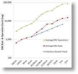
However, as design processes became more and more complex, the number and complexity of the rules required per node continued to increase (Fig. 3). In addition, the amount of hard intellectual property (IP) that was being reused increased significantly. Thus, the waiver process became unwieldy, particularly for the designer.
3. The number and complexity of design rules increases at each new node.
IP Error Waiving
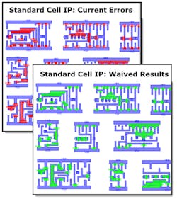
In particular, when a piece of IP contains an error that’s known to be waivable, having to review each placement of that IP in each new design becomes an exercise in frustration and wasted time. To combat this issue, a new bottom-up approach for IP waiving was introduced, in which waivers for a given IP and a given process are captured once. As that IP is reused, the waiver is preserved with the IP. Any chip designers who use that IP know they can safely ignore the waived errors and focus on fixing real errors introduced at the time of floorplanning and block placement (Fig. 4).
4. The bottom-up approach to waivers management preserves waiver information with a piece of IP.
While this approach seems intuitive, it also creates a new set of issues. If we’re keeping waivers associated with a piece of IP for a long time, how do we know we can still trust them? Who waived them? When and for what reason? Did anyone else review and approve the waiver? Has the IP changed since the waiver was created? Has the rule file it was associated with changed?
These concerns led to an ever-growing infrastructure to ensure that no real IP error is ever incorrectly waived. Electronic-design-automation (EDA) software tools can now automatically capture a snapshot of the IP, its waivers, and the associated rules, and embed that data with the waivers and/or the IP.1,2 With this information readily available, users can be alerted to unexpected changes. Similarly, waivers can be tagged with information describing their initial creation. By searching and filtering on this information, CAD teams or other design infrastructure teams can quickly search out waivers of concern.
Not-So-Hard IP
Another issue with IP waivers stems from the fact that not all IP is hard IP. For example, consider the SRAM, a mainstay in IC design. It’s highly unlikely that designers today would instantiate an off-the-shelf SRAM. Rather, they use an SRAM compiler containing a set of input pieces: bit cells, IO cells, periphery blocks, etc. This approach allows designers to create legal SRAMs of various sizes to meet their needs.
But, because these created SRAMs did not exist as standalone IP before they were compiled, there’s no way to capture the waivable errors associated with them. This is particularly troublesome because SRAMs are a known design type that can intentionally break traditional design rules. Traditional rule-based methods to waive these errors are risky, as they tend to mask all errors associated with the SRAM, including any real errors introduced at placement time.
Fortunately, there’s a solution for these IP as well. EDA tools can capture and store typical patterns of legal SRAM configurations (e.g., bit-to-bit, bit-to-IO, …). Designers can then check their corresponding compiled SRAMs against these configurations to validate that the compiled IP were actually created and placed without introducing new errors. The same methodology can then be used to indicate that known errors associated to these configurations are able to be safely waived.3
One final issue with the bottom-up waiving methodology is that it assumes all inputs to a design level are fully complete and their waivers have been captured before running the next level up. For design teams under a tight time-to-market window (that would be every design team in the known universe), this assumption isn’t practical. Decisions on floorplanning and placement are made far ahead of the blocks’ final layout, and chip-level routing takes place before the block-level layout is DRC-clean. So how can the chip-level designer properly debug the placements and routing without being hindered by the errors associated with incomplete or incorrect block layout?
It’s impractical to run each of these early block versions just to capture and waive their errors one by one, because the vast majority of these errors will be fixed before final tapeout. Thus, an early waiver run provides neither value nor useful data. For this use case, a form of temporary waiving is needed. By relying on the cell name or blocking regions, the bottom-up waiving approach can be easily used to temporarily waive all of the errors in the specified region at chip-level runtime.
Looking Ahead
The more we learn about design layout, the more complicated it seems to become. Fortunately, just like a woodworker’s ability to tailor the construction process to the demands of each project, our ability to quickly and safely identify DRC errors that don’t require fixing is also constantly growing and improving to meet the new challenges presented with each new node and technology.
What waiver challenges will the future of IC design bring? Multi-chip heterogeneous packages? Optical signal processing? Thermal impacts and tuning? Whatever the case may be, rest assured that engineers are working now to ensure that we understand and are able to provide the technology needed to precisely and correctly identify and waive errors in these designs.
John Ferguson is Director of Marketing for Calibre DRC applications at Mentor, a Siemens Business. John has extensive experience in the area of physical design verification. He holds a B.Sc. degree in Physics from McGill University, an M.Sc. in Applied Physics from the University of Massachusetts, and a PhD in Electrical Engineering from the Oregon Graduate Institute of Science and Technology.
References:
1. Paris, James, “Physical IP waiver management with Calibre Auto-Waivers,” Mentor, a Siemens Business. May 2016.
2. Ferguson, John, “Automated DRC Waiver Management for IP Block Integration,” Mentor, a Siemens Business. June 2009.
3. Paris, James, “Dynamic Waiver methodology with Calibre Pattern matching,” Mentor, a Siemens Business. May 2016.


