Micro-electromechanical systems (MEMS) represent a key technology in the measurement space. Whether you are looking to design, produce, and test your own MEMS and associated circuitry or develop a MEMS-based system based on commercially available processors and sensors, you’ll find products introduced over the past few months that support your efforts.
For example, Coventor has released a new version of its co-design platform for MEMS and ASIC development, Advantest announced an electron-beam lithography system that supports MEMS and related nanoscale fabrication processes, Si-Ware Systems developed an ASIC for use with Tronics’ new GYPRO2300 Gyrometer, STMicroelectronics has a development platform with build-in MEMS sensors, and Multitest announced that its MT9928 Test Handler supports MEMS oscillator test.
MEMS Design Automation
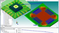
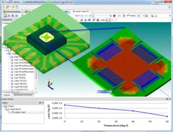
In November, Coventor, a supplier of design-automation software for developing MEMS products, introduced its MEMS+ 3.0 design platform (Figure 1). This latest version targets the development of complex 3-D systems with state-of-the-art actuators, accelerometers and gyroscopes, microphones, and other types of MEMS devices.
Courtesy of Coventor
The company reported that the MEMS+ 3.0 platform delivers improvements for simulating the dynamics of MEMS actuators and sensors, adds new components for modeling a wider range of MEMS designs, and provides speed and capacity improvements. The new capabilities enable MEMS designers to explore device concepts and optimize designs faster than using conventional field solvers. The company reported that most simulations run in seconds or minutes rather than hours or days.
The MEMS+ platform also eliminates months of engineering effort required to handcraft the models for IC simulation with a common model for MEMS and ASIC co-design that bridges the gap between the accuracy required by MEMS designers and the simulation speed required by ASIC designers.
The company reported that MEMS-based products typically include one or more MEMS devices fabricated with a specialized process, an ASIC fabricated with a standard CMOS semiconductor process, and a package. For development of these devices, MEMS and ASIC designers use different, incompatible tool chains that result in multiple design respins with the ASIC design lagging the MEMS design by nine to 18 months due to inefficient communications.
Speaking at the time of the platform’s introduction,1 Coventor CEO Mike Jamiolkowski said, “Coventor’s MEMS+ changes the design paradigm. It’s a unique platform that enables truly integrated MEMS and ASIC co-design and verification. MEMS+ 3.0 adds major new advancements for simulating complex coupling dynamics among MEMS, ASIC, and packaging with a speed and capacity that’s not available from other tools.”
“The MEMS+ solution provides us with an excellent platform to design MEMS in the context of the IC and other systems we are developing,” said Anssi Blomqvist, senior manager for product development at Murata Electronics, in a press release. “The integration with the other design tools in our environment enables a seamless exchange between the different design domains. We look forward to leveraging the enhancements in the new release that improve the overall performance of the tool and add new modeling capabilities for micromechanical effects which are important to us.”
The MEMS+ 3.0 platform leverages more than a decade of industry experience with Coventor’s Architect3D and CoventorWare products for 3-D design entry and simulation. Its tight integration with MATLAB and Simulink from MathWorks and the Virtuoso Custom IC design solution from Cadence Design Systems provides a robust environment for simulating the complex physics of MEMS devices together with IC circuits and control systems, the company reported.
The new release offers an enlarged, comprehensive MEMS component library and new fluidic simulation capabilities that include gas damping for sensors and actuators and pressure loads for microphones. The addition of fluidics to the existing mechanical and electrostatic modeling capabilities platform enables fully coupled simulations that predict performance metrics like noise or actuation time previously done through costly build and test cycles. In addition, the capability to selectively linearize compute-intensive portions of MEMS models provides greater speed, which is critical during the initial phases of MEMS and IC co-simulation.
“As a long-time user of Coventor’s Architect3D and Analyzer products, I am excited to see the latest release will include new brick and shell elements, Timoshenko beams, squeeze film damping, and packaging effects. These new features will enable more accurate and thorough exploration of the dynamic behavior of our MEMS devices prior to prototyping,” commented Jonathan Hammond, principal engineer at RF Micro Devices, in a press release.
Other advancements incorporate improved Cadence design tool integration that provides true multiphysics simulation in the Virtuoso environment and MEMS+ model support for the multithreaded spice APS simulator, complete multiphysics input/output and full scripting interface support in the MATLAB environment, and a new built-in simulator that handles basic MEMS analysis tasks.
MEMS Production
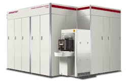
Advantest announced in November that it has developed a new electron beam (EB) lithography system, the F7000, with resolution performance meeting the requirements for 1Xnm technology nodes (Figure 2). The F7000 supports substrates of diverse materials, sizes, and shapes, including nanoimprint templates as well as wafers, and is optimized for diverse applications such as advanced LSI, photonics, MEMS, and other devices fabricated using nanoprocesses.
Courtesy of Advantest
Advantest said that competition in the mobile electronics and other categories has sparked an urgent need for chip makers to develop increasingly low-power, highly functional semiconductors while reducing time to market. As a result, manufacturers are looking to EB lithography, which writes fine-pitch patterns directly onto wafers, as a method of accelerating cutting-edge semiconductor R&D processes.
Advantest’s new F7000 offers the company’s EB technology in a system capable of writing patterns as fine as 1Xnm. The system also supports template fabrication for nanoimprint lithography—a technology positioned to take center stage in next-generation semiconductor manufacturing, the company said.
The product achieves its 1Xnm resolution performance by using a new column technology. The F7000’s adjuster function enables it to handle diverse sizes of wafers, glass substrates, and square substrates. By switching adjusters, the system can support silicon, gallium arsenide, and substrates of other materials utilizing separate adjusters for each material to avoid contamination. Users can select standalone or in-line configurations to support a variety of applications from R&D to volume production. Advantest said the new system achieves a write speed five times faster than its predecessor model, the F3000, while occupying a 40% smaller footprint.
Development Platform
Also in November, Si-Ware Systems (SWS), a provider of IC- and MEMS-based products for industrial and consumer applications, announced it has developed and is supplying a conditioning ASIC for Tronics’ new GYPRO2300 Gyrometer. The SWS conditioning ASIC along with the Tronics MEMS element produces a gyroscope that has a bias instability (Allen variance) of 1° per hour, a low noise density, and a thermal bias stability of ±0.05° per second.
SWS said it worked closely with Tronics on the integration and industrialization of the gyroscope module. It also supported Tronics in the characterization of its MEMS gyroscope, which was enabled through SWS’s MEMS development platforms, allowing for a better understanding of a MEMS device and its behavior with interface electronics.
SWS’s most recent inertial sensor development platform is the SWS61111, which permits companies themselves to characterize their MEMS sensors at an early stage. The SWS61111 utilizes SWS’s high-performance inertial sensor interface ASIC, the SWS1110. The SWS1110 is a highly configurable ASIC that can be interfaced with accelerometers and gyroscopes in open- and closed-loop (force-feedback) operation.
SWS’s SWS61111 is designed to accommodate quick and easy interfacing of almost all capacitive MEMS devices. MEMS and ASIC designers can evaluate issues such as parasitic modes of oscillation, electrical and mechanical coupling, high-voltage effects, and temperature behaviors. It also serves as a tool to evaluate SWS’s SWS1110 high-performance ASIC, which is offered in die format with optional customization, for product targeting the high-end segment.
The SWS61111 consists of a programming board, an ASIC daughter board with a sensor placeholder, a USB interface, and associated PC software. SWS provides options for mounting the sensor to the daughter board, including creating custom daughter boards to match a particular sensor. Through an easy-to-use software interface, the MEMS sensor can be interrogated and the ASIC parameters configured to best match the sensor. If desired, the ASIC parameters then can be burned into the memory of the ASIC, and the sensor-ASIC daughter board can be removed and utilized for system-level measurements.
In addition to its experience with MEMS inertial sensors, SWS said it has worked with piezoelectric sensors, MEMS resonators, and MEMS optics and developed an extensive IP library of electronics for MEMS and piezoelectric devices that can be utilized in the development of interface ASICs.
MEMS Development Kit
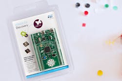
STMicroelectronics also is supporting MEMS interfacing and has released an easy-access development platform (Figure 3) for projects based on its new high-performance STM32 F3 Microcontrollers, which now are starting to enter volume production.
Courtesy of STMicroelectronics
The new development platform, the STM32 F3 Discovery Kit, features built-in MEMS sensors—a gyroscope and e-compass—with nine degrees of freedom (three axes of linear motion plus three axes of angular motion plus three axes of magnetic motion), enabling competitively priced sensor-fusion applications, such as implementation of Attitude Heading Reference Systems (AHRS). ST’s e-compass or geomagnetic module integrates a three-axis digital magnetometer with a three-axis digital accelerometer used for tilt compensation. AHRS systems provide attitude and heading information using gyroscope, magnetometer, and accelerometer measurements for calculating 3-D orientation with a dedicated algorithm.
Sensor fusion and the microcontroller’s computational capabilities enable designers to realize advanced 3-D motion-sensing systems in applications such as mobile gaming, augmented reality, optical image stabilization, portable navigation, robotics, and industrial automated systems.
The STM32 F3 Discovery Kit includes a ready-to-use prototype board containing an STM32F303 Microcontroller and associated chips as well as indicator LEDs, push-button controls, I/O pin headers, and a USB connection for the host PC. All of the microcontroller pins are brought out to accessible points to aid testing and debugging. The MEMS devices provided on the board are the L3GD20 three-axis digital gyroscope and LSM303DLHC six-axis geomagnetic module from ST’s MEMS portfolio of sensors and iNEMO inertial modules. The STM32 F3 Discovery Kit is compatible with STM32 software-development environments from third-party vendors including Altium, Atollic, IAR Systems, and Keil.
The STM32F30x microcontrollers combine the high computational resources of the ARM Cortex-M4 Processor, which has a DSP and floating-point unit, with advanced peripherals. When used with MEMS sensors in high-performance sensor-fusion applications, the processor can perform floating-point matrix operations for efficient execution of 3-D orientation functions such as AHRS algorithms.
The peripherals available in STM32F30x devices include four 12-bit 5-MS/s ADCs. Also on-chip are seven 50-ns comparators, four programmable-gain amplifiers with 1% accuracy, two 12-bit DACs, and two advanced timers that can control two motors simultaneously or be used in applications such as digital power supplies, data servers, or solar micro-inverters.
The STM32F37x series peripherals include the first 16-bit sigma-delta ADC integrated in an ST microcontroller. Devices in the series feature up to three of these ADCs, providing the basis of a single-chip solution to replace a discrete general-purpose processor and separate ADC for high-precision sensing applications. The STM32F3 Discovery Kit has a recommended resale price of $10.90.
Test Handling
When it comes to testing MEMS devices, the electrical requirements don’t differ much from the electrical test requirements of other devices. In fact, National Instruments’ MEMS test web page provides links to tutorials and sample programs on several general-purpose test topics, including opens and shorts testing,2 power consumption testing,3 JTAG protocol implementation,4 and serial-bus implementations.5
Test handling, however, is a different story. To that end, in December, Multitest announced that its equipment fully supports the MEMS oscillators. MEMS oscillators are considered to be a favorable alternative to the long-established, quartz crystal oscillator technology. Today they represent approximately 1% of the timing market, but significant growth is expected in the future.
Besides performance, reliability, and the more comprehensive features, the company said, one substantial advantage is that packaging and test are very similar to standard IC processes. Economy of scale can be achieved. This significantly contributes to the favorable cost structure, price, and availability.
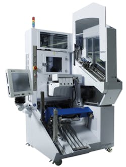
Multitest’s standard MT9928 Test Handler (Figure 4) has been deployed for calibrating and trimming MEMS oscillators at various customers. All systems were delivered as full Plug&Yield solutions, including the Multitest conversion kit, Multitest socket, and Multitest load board. All typical packages sizes of MEMS oscillators are supported.
The MT9928 Gravity Feed Handler ensures the required temperature accuracy (up to ±0.2°K) but also provides high throughput and low cost of test. This way, the test handler fully supports the favorable cost structure.
Courtesy of Multitest
The MT9928 xm is a well-established, user-friendly, and easy-to-maintain platform. Additionally, the unique Multitest Plug&Yield program delivers a fully integrated solution with all components harmonized, configured, and finally, checked at system level. As a result, the MT9928 also is a good solution for companies that are not overly familiar with the standard IC test process.
Looking Ahead
MEMS will continue to be a focus of companies ranging from design-automation firms to device vendors and test-equipment manufacturers. The 2013 Semicon West show (July 9-11 in San Francisco) may prove to be a venue for highlighting recent advances—MEMS will be among many topics of interest at the show.
SEMI, the show organizer, is soliciting technical papers for an extreme electronics track on MEMS manufacturing and technology. MEMS-related presentations also might be appropriate for a packaging and test track, for which SEMI is soliciting papers on semiconductor test strategies, trends, and opportunities in 3-D ICs; advanced packaging materials and technologies; and probe-card technology.
SEMI invites prospective presenters to submit abstracts (maximum 500 words). The deadline for abstract submission is March 1.
References
1. “Coventor Debuts MEMS Plus IC Co-Design Software,” EE-Evaluation Engineering Online, Nov. 18, 2012.
2. Opens and Shorts Testing Reference Design, National Instruments, Tutorial, Oct. 10, 2011.
3. Power Consumption Testing Technical Details (IDD, IDDQ), National Instruments, Example Program, Nov. 7, 2009.
4. JTAG Digital Waveform Reference Library, National Instruments, Example Program, Sept. 8, 2011.
5. SPI Digital Waveform Reference Library, Example Program, National Instruments, Example Program, Sept. 8, 2011.
For Further Reading
Lecklider, T., “Maintaining a Set Course,” EE-Evaluation Engineering, September 2012.
Nelson, R., “Community College Boosts MEMS Commercialization,” EE-Evaluation Engineering Online, Aug. 5, 2012.
Nelson, R., “Driving MEMS Commercialization,” EE-Evaluation Engineering, September 2012.
Nelson, R., “MEMS technology roadmapping could address test challenges,” EE-Evaluation Engineering Online, July 23, 2012.
Nelson, R., “Modular Instruments Address IC Test,” EE-Evaluation Engineering, July 2012.
Nelson, R., “Vendors Explore Data-Capture Options,” EE-Evaluation Engineering, December 2012, p. 14.
Vranes, M., “Designing a MEMS Test System: Tips and Techniques,” MEPTEC Report, Fall 2012, p. 12.
