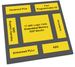
Developers can take advantage of the low-power or high-performance mode. There’s a mix of DSP blocks, embedded memory, and up to 40K logic cells. Off-chip DDR3 memory is accessible via a 1066-Mb/s interface; differential I/O SERDES work up to 1.5 Gb/s. LVDS and subLVDS interfaces are supported. Versions are available with an ADC, too.
The instant-on operation of the chips allows I/O to be configured within 3 ms. Total device configuration takes 8 to 14 ms.
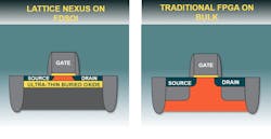
The Certus-NX is the second Nexus architecture solution from Lattice (Fig. 2). The initial version was the CrosssLink-NX. The Nexus platform is based on fully depleted silicon-on-insulator (FDSOI); the FD-SOI support comes from Samsung. It reduces transistor leakage in half versus bulk CMOS.
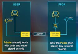
The Certus-NX will be used in a range of applications, including connected IoT solutions. On-chip security support allows a public key to be stored to verify information coming from outside (Fig. 3); the Elliptic Curve Digital Signature Algorithm (ECDSA) is used for this purpose. The chips also support AES-256 encryption.
The Certus-NX comes in package sizes ranging from a 6- × 6-mm csfBGA to 14- × 14-mm csfBGA. The compact layout delivers twice the number of I/O pins in these form factors.
Lattice’s Radiant software-development suite supports the Certus-NX as well as its other FPGA solutions like the CrossLink-NX. Certus-NX also works with Lattice’s SensAI. The SensAI tools provide machine-learning (ML) support, including FPGA-based binarized-neural-network (BNN) and convolutional-neural-network (CNN) acceleration. The SensAI neural-network compiler can accept models from frameworks like Caffe and TensorFlow.


