Minimize Write Amplification to Maximize Storage-System Lifetime
What you’ll learn:
- How to maximize storage life by decreasing write amplification factor (WAF).
- How the address-mapping choice can make a big difference to the WAF.
- How the appropriate flash-management firmware can assist with the above.
Flash memory is organized in a hierarchy of blocks, pages, and cells. In the older single-level-cell (SLC) devices, each cell stores only one bit of information. With the newer multi-level-cell (MLC) memory, pages are typically between 8 and 16 kB. Blocks can be up to 8 MB.
When it comes to NAND flash, data is written a page at a time. However, only whole blocks can be erased. To ensure this is carried out correctly, the flash controller uses mapping algorithms to process exactly where data should be sent on the NAND flash.
This mapping data manages the blocks and pages and allocates them for subsequent use. Flash-controller mapping involves lots of complex algorithms and ultimately ensures that wear and tear is carried out evenly. If wear occurs evenly, it helps ensure drive longevity and optimizes flash management.
Write Amplification Factor
Rewriting data to an SSD significantly affects endurance. An important parameter for tracking the lifetime and endurance of a storage device is the write amplification factor (WAF). There’s one important element to remember with the WAF: the smaller, the better.
The WAF tallies the number of writes made to the flash memory and then performed by the host. Extra writes may be needed for functions such as erasing blocks before data is written. The extra writes could indicate a mismatch between the data amount and the page size.
For example, a sequential write of 4 kB of data to a flash memory where the page size is 16 kB will result in a WAF of 4, because the entire page must be written (4 kB four times in a row to total 16 kB). Since a partial block erase isn’t possible, it’s important for the algorithm to take the mapping of the whole block into consideration.
Block-Based mapping
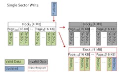
In any flash storage system, the controller must manage the mapping from the logical addresses used by the host operating system to flash memory physical addresses. A simple, however arguably outdated, method commonly used is block-based mapping, in which a one-to-one mapping occurs between addresses within logical and physical blocks (Fig. 1).
Managing in this way causes logical page 1 to always map to physical page 1 in a block, although this can be in any block.
The address-mapping choice can make a big difference to the WAF. In the case of block-based mapping, write amplification can be enormous, especially for small random writes. If a block must be erased to accommodate a single sector write, the WAF can increase to 2000 because adding the new data initiates copying the entire block of previous content to a new block.
Certain SD cards designed for video recording still use block-based mapping due to the data patterns that involve many sequential writes and only erasing data once the card is written full. However, most applications have a greater need for performance.
Sub-Page Mapping
Page-based mapping is a more versatile logical-to-physical address-mapping method than block-based mapping. While logical pages are still mapped to physical pages, more flexibility is available because logical page 1 can now be mapped to any physical page within a block.
Sub-page-based mapping means that the address mapping is achieved at a level smaller than a page. Memory-allocation flexibility broadens with this technique. However, writes still must be done at the level of an entire page.
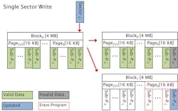
Sub-page-based mapping significantly reduces the WAF. Even if a block has to be erased because no unused block is available, only the new sector of data must be written to the new block. The old sector of data is marked as invalid, and the other data in that block stays put.
As a result, even in the worst-case scenario, the WAF is reduced to 16 compared with the 2000 mentioned earlier. By reducing the number of extra writes, sub-page-based mapping can significantly improve the lifetime of a drive.
For example, Hyperstone’s flash-management firmware, hyMap, implements an enhanced Flash Translation Layer (FTL) mapping that improves random write performance, reliability, and endurance (Fig. 2). Since many factors including the pattern of use affect the overall WAF, firmware can be compiled for different sub-page granularities and tuned to the expected usage model.
By increasing drive endurance and longevity, hyMap firmware and its sub-page-based mapping system enables cost savings in applications that have replaced older SLC designs with MLC memory designs.
Continuously optimizing flash-memory-controller mapping ensures higher performance, a lower WAF, and increased endurance. As a result, cost reduction, higher capacity, and greater competitiveness is possible.
Damien Col is Technical Marketing Manager at Hyperstone.


