This article appeared in Microwaves & RF and has been published here with permission.
You’ve finally completed your printed-circuit-board (PCB) design for a new product. You run your design-rule checks and some sort of generic design-for-manufacturing (DFM) check, and the report says the design is clean. All good, right? Most likely, probably not. When your PCB house gets its hands on the design, it runs its own checks and comes up with several issues that make your board a problem child.
Why does this happen? It’s most likely because your DFM tool is blissfully unaware of your PCB house’s true manufacturing constraints. There’s a yawning gap between the design and manufacturing ecosystems, and Siemens aims to close it with PCBflow, a cloud-based software solution. PCBflow extends Siemens’ Xcelerator portfolio with a secure environment PCB design teams to interact with a variety of manufacturers. By rapidly performing a range of DFM analyses in the context of each manufacturers’ process capabilities, the software helps customers accelerate design-to-production handoff.
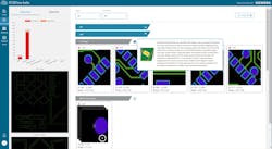
Thanks to its underlying Valor NPI software engine, which performs over 1000 DFM checks, PCBflow enables PCB design teams to rapidly identify manufacturability violations (see figure). These violations are then sorted and prioritized according to level of severity, guiding users through images and locations on the design for easy identification and immediate correction.
The idea behind PCBflow is collaboration. Its success will, in the end, depend on the PCB fabrication houses securely uploading their sets of manufacturing constraints to the cloud. With that done, the software supports comprehensive collaboration between designers and manufacturers with a closed-loop feedback mechanism that drives continuous improvement. Ideally, it means that the days of PCB respins are in the rearview mirror. In practice, if it results in designers getting closer to a first-spin success, it’s a win-win for both parties. With the design being in sync with the fabricator’s capabilities, time to market shrinks, board quality is optimized, and fabrication yields are improved.
For manufacturers, PCBflow gets design teams onboard with their process faster while providing them with comprehensive process knowledge. Because the PCB maker’s manufacturing capabilities are shared electronically, it cuts down on the long phone calls and email exchanges that are part of the debugging process. Because designers are proactively addressing process violations during the design process, the fab house has more time to focus on more valuable discussions.
Engineered for ease-of-use, PCBflow requires neither training nor prerequisites, and it is accessible from virtually any location, including mobile phones and tablets. Additionally, PCBflow provides designers with images, tool tips, measurements, and precise locations of solderability issues and other PCB design violations. Reports are available online and in a downloadable PDF format for easy sharing. PCBflow supports the ODB++ language design file format and support for additional formats is planned in 2021.
As a software as a service (SaaS) technology, PCBflow incorporates the strict security standards of Siemens’ software, reducing risk and protecting intellectual property (IP) with no additional IT investment. The PCB design team doesn't need to see the fabricator's design constraints if that's the way they want to go.
Finally, PCBflow works with the Mendix low-code application development platform. The platform provides the ability to build multi-experience apps and share data from any location, on any device, on any cloud or platform, to realize the benefits of digital transformation more quickly.


