How Can Pseudo-SLC Combine Both Longevity and Economy?
What you'll learn:
- Comparison of NAND flash level-cell types.
- What are the benefits of pseudo-SLC versus TLC and the others?
- How pSLC creates new storage capacities.
Today's NAND flash technology industry is awash with success stories about reaching new memory densities. The technology has long since achieved well over 100 layers, and there seems to be no limit anytime soon.
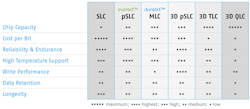
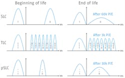
The steady increase in the number of layers goes hand in hand with the trend to store more bits per cell. The current mainstream technology is triple-level cell (TLC). It stores three bits per cell, where the term “level” refers to the number of bits, not the internal states. The number of internal states that need to be safely stored and read again are to the power of two of the number of bits stored, meaning that with three bits, eight different states need to be recognized. The trend is toward even more memory for the same chip size, which is realized by quad-level cell (QLC), four bits per cell, which has the demanding task of managing 16 states.
The increasing amount of stored information per square centimeter of silicon will decrease the number of feasible write cycles. While with single-level cell (SLC), one bit per cell, it was still possible to rewrite each cell 60,000 to 100,000 times, with multi-level cell (MLC), two bits per cell, the number was reduced to 3,000.
In the transition from planar MLC to 3D TLC (two versus three bits), it proved possible to maintain the 3,000-cycle life due to the better cell properties with 3D charge trap flash. This value is reduced to around 1,000 with QLC and to a value of less than 100 with the next evolutionary stage: penta-level cell (PLC), five bits per cell = 32 states.
PLC is no longer at the prototype stage. In time, it will become the mainstream NAND for hyperscale data-center applications, such as those at Google or Facebook, where data is only written once and read frequently—write once, read multiple (WORM).
High Demands Have Their Price
In contrast, applications remain that write vast amounts of small data, be it the recording of sensor data, local IoT databases, or the recording of status information. Writing small packets in the byte to kilobyte range wears out NAND flash far more quickly than data transfers in the megabyte range.
For these applications, SLC was previously the best storage medium. Due to small block sizes and up to 100,000 possible erase cycles, SLC-based memory modules are often more durable than the required operating life in the field. In addition, SLC is less temperature-sensitive and has lower requirements for error correction in the controller, all of which has a positive impact on long-term performance.
However, the main reason for replacing SLC in these demanding applications is down to another important consideration—price. SLC technology suffers from the “chicken-and-egg” dilemma: Due to the older, more expensive technology, the mainstream is gradually moving away from SLC, which is why it’s not worth transferring SLC to more modern technology.
Pseudo-SLC as an Attractive Middle Ground
Today's SLC technology has a maximum capacity per chip of 32 Gb with a typical chip area of 100 mm². A common and similarly priced 3D NAND TLC chip, on the other hand, has 512-Gb capacity and in the next generation will reach 1 Tb. It makes TLC technology 16 times less expensive than SLC.
This effect is put into perspective at the system level: TLC controllers are more complex and more expensive, and with 512-Gb NAND chips, the minimum capacity of a drive is equal to 32 GB. This isn’t a problem for data centers or ambitious home users. In these scenarios, interesting drive sizes tend to start beyond 1 TB anyway. However, the situation is different for applications in the industrial sector or as a boot drive for network or communication systems. In these cases, a few gigabytes, albeit used more intensively, is usually sufficient.
Since only one chip is used in the 32-GB TLC case described above, the drive offers a rather low write and read speed, regardless of its interface, because the system performance results from the number of parallel flash channels—the more channels that are equipped, the higher the performance. High-speed SSDs use up to 16 parallel flash channels to achieve the corresponding performance. With several parallel SLC flash chips, a fast SSD also can be realized with much smaller capacities.
What would be desirable is an SLC chip with modern 3D NAND technology that’s manufactured in high volume and is consequently cost-effective. Remembering the definition of SLC (i.e., one bit per cell), it’s indeed feasible with all modern NAND flash products. However, the internal controller must be told to work with only two states: erased and programmed; 1 or 0. This mode of operation is called pSLC or pseudo-SLC.
The Advantages Do Outweigh the Disadvantages
By using only two internal states, programming can be achieved with a lower voltage. This protects the sensitive silicon oxide in the memory transistor and extends its life. Since the electronics must only distinguish between two states, the signal-to-noise ratio is much greater than in cases where 32 states are present. Degradation of the stored value can be tolerated much longer than with TLC or QLC.
Both effects mean that the permitted number of programming or erasing cycles increases from 3,000 for TLC to a figure between 30,000 and 60,000 for pSLC. It brings this operating mode back into the range of “real” SLC technology.
2D MLC NAND also has been able to operate in pSLC mode. Here, only one of the two bits per cell was used, thus halving the capacity. Writing only one bit also delivered speed advantages. Costs per bit doubled, of course, since only half the bit capacity was available per silicon chip.
With TLC technology, only one of three bits per cell is used. Therefore, the cost triples to achieve the same storage capacity. Nonetheless, this is still much cheaper than with real SLC NAND.
Using QLC in pSLC mode, on the other hand, offers no advantage. QLC has 1.33X the capacity of TLC, but you only use a quarter of the bits per cell. As a result, the pSLC capacity is identical for QLC and TLC.
pSLC Leads to “New” Storage Capacities
Reducing the chip capacity to one third has an unusual effect on the commonly used SSD capacities. In the binary IT world, people were accustomed to calculating with multiples of two: 64, 128, 256, 512, etc., GB drive capacity.
However, with the transition to 3D NAND, more memory was needed internally to realize caches or RAID, or so-called overprovisioning, where extra reserved memory is used to speed up writes and increase lifetime. The resulting capacities are then 30, 60, 120, 240, 480, etc., GB.
Such capacity available to the user is indicated by the parameter “User LBA Range.” It’s often seen in the specifications of SSDs that claim “binary sizes,” where the “User LBA Range” actually has been reduced to exactly this extent. In such a case, the drive shows 512 GB, but the user only has 480 GB available. Caution is advised here, as manufacturer specifications with this level of detail are quite rare, such that the actual capacity is often only discovered during operation.
If the pSLC reduction is now added, it results in unusual new drive sizes: a 480-GB TLC SSD becomes a 160-GB pSLC SSD, which is as expensive as a 480-GB TLC SSD. Customers from the embedded or network and communication sectors who use fixed images of their system environment still use binary sizes for small capacities. For these cases, the user capacity is then reduced to the next smaller binary capacity, with the advantage that the service life is once again disproportionately larger. However, the price per gigabyte of usable capacity also increases slightly.
Conclusion
pSLC optimally complements classic SLC memory technology and is an ideal solution for cost-effectively adapting 3D NAND technology to the lifetime of SLC. The only disadvantage is the unfamiliar new drive sizes like 10, 20, 40, 80, and 160 GB.
For this reason, industrial memory manufacturer Swissbit also offers the option of pSLC mode for almost all products with MLC and 3D TLC NAND. True SLC products will remain in the company’s range in the long term because the advantage of true SLC is the fact that it no longer needs changing every two years, thereby saving the costs of requalification. For markets like medical technology, automation, or transportation with very long product life cycles and onerous standardization requirements, there’s still no alternative to real SLC. That’s why it’s important to have a reliable memory partner with long-term customer solutions.


