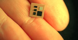
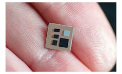
Silicon interposer technology allows multiple die to be combined onto a single chip. This is different from stack or multi-die chips that use wires to connect to a substrate. Essentially, the interposer is similar to a printed circuit board (PCB), but on a much smaller scale.
Silicon interposers used to be exotic technology, but they have become more common as fabrication practices have improved. It was used in high-end FPGA solutions like Xilinx’s Virtex-7 2000T where it delivered 10,000 connections between multiple die in a 2.5D architecture. Altera used a slightly different approach to link its high-speed serial interfaces to the FPGA fabric.
Silicon interposer system design tends to be less complex that an SoC design, but it is still a challenge. Up until now it hasn’t put the technology into the same realm as PCB design, but a company called zGlue is looking to change this—at least on a small scale.
zGlue has developed a programmable silicon interposer fabric that targets compact applications (e.g., wearable tech) that includes applications such as medical devices. It allows developers to combine die onto the fabric, resulting in a much smaller compact form factor. The programmability of the underlying structure speeds the implementation process allowing chips to be delivered in as little as eight weeks while reducing the form factor by a factor of 10.
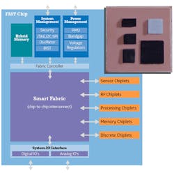
The zGlue interposer comes in one size at this point, but it can be used for any number of die that will fit on it. Developers can provide their own and work with zGlue to incorporate them into a chip, or they can take advantage of BGA “chiplets” that are die already approved by zGlue (Fig. 2). These include a range of sensors, microcontrollers, memory, and even RF technology like Bluetooth or cellular chiplets. They hybrid memory is used for configuration data, system test support, as well as secure key storage. Memory can also be supplied as a chiplet or as part of other devices like the microcontroller chiplets.
The ZiP platform can employ a number of analog and digital ports—up to 20 of each. The system also comes with zGlue’s system and power management support. The power management support allows operation with a range of batteries, including lithium and NiCads, as well as low-voltage supplies. Systems have built-in voltage regulators. Eventually gGlue will have a zGlue ZiPlet Store where developers can pick and choose chiplets.
The current configurations provide a working area up to 48 mm2 and 20 I/O pins. Standard external interfaces include I2C, SPI, UART, and GPIO. Analog/RF connections up to 2.4 GHz are supported. The interconnect fabric supports up to 3 K connections.
At this point zGlue handles most of the system configuration versus using an FPGA- or PCB-style layout tool. Developers typically come to zGlue with a block diagram or an existing PCB layout that will be converted into a single chip.
It is possible to perform similar tricks found in PCB designs—such as laying out larger spaces for a chiplet—so that larger, typically higher-capacity or -performance chiplets can be utilized in additional products. This is a common methodology when companies need to deliver a range of products with increasing levels of functionality, capacity, or performance.
zGlue’s platform is not a fit for all compact embedded applications, but it can be a significant advantage for those where small, custom configurations are needed. It is significantly less costly than creating a custom SoC while providing similar flexibility when the appropriate chiplets are available.
About the Author
William G. Wong
Senior Content Director - Electronic Design and Microwaves & RF
I am Editor of Electronic Design focusing on embedded, software, and systems. As Senior Content Director, I also manage Microwaves & RF and I work with a great team of editors to provide engineers, programmers, developers and technical managers with interesting and useful articles and videos on a regular basis. Check out our free newsletters to see the latest content.
You can send press releases for new products for possible coverage on the website. I am also interested in receiving contributed articles for publishing on our website. Use our template and send to me along with a signed release form.
Check out my blog, AltEmbedded on Electronic Design, as well as his latest articles on this site that are listed below.
You can visit my social media via these links:
- AltEmbedded on Electronic Design
- Bill Wong on Facebook
- @AltEmbedded on Twitter
- Bill Wong on LinkedIn
I earned a Bachelor of Electrical Engineering at the Georgia Institute of Technology and a Masters in Computer Science from Rutgers University. I still do a bit of programming using everything from C and C++ to Rust and Ada/SPARK. I do a bit of PHP programming for Drupal websites. I have posted a few Drupal modules.
I still get a hand on software and electronic hardware. Some of this can be found on our Kit Close-Up video series. You can also see me on many of our TechXchange Talk videos. I am interested in a range of projects from robotics to artificial intelligence.
Voice Your Opinion!
To join the conversation, and become an exclusive member of Electronic Design, create an account today!

Leaders relevant to this article:


