System-on-module (SOM) and system-in-package (SIP) solutions were out in force at this year’s Embedded World. These cost a bit more than trying to put comparable logic down on a printed circuit board (PCB), but most will likely result in lower-cost solutions that are more flexible and powerful.
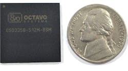
Take, for example, Octavo Systems’ OSD335X-SM SIP design (Fig. 1). It packs in more than 100 components including a 1-GHz Texas Instruments Sitara AM335x ARM Cortex-A8 Processor, up to 1 GB of DDR3L memory, a TPS65217C power-management IC (PMIC), a TL5209 LDO regulator, a 4- kB EEPROM, and all necessary passives into a 21- by 21-mm, BGA. The AM335x can run Linux and includes a touchscreen display controller with a 3D PowerVR SGX graphics system; USB OTG with PHY; dual Gigabit Ethernet; an 8-channel, 12-bit SAR ADC; and a programmable real-time unit (PRU) that allows the network to support protocols like EtherCAT.
1. Octavo Systems’ OSD335X-SM packs an entire system into a compact SIP.
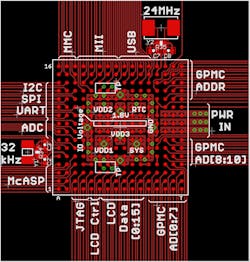
The OSD335X-SM groups signals to simplify PCB layout (Fig. 2). It has 16- by 16-ball grid with a 1.27-mm pitch that allows routing on a single side of a PCB. This allows the SIP to be used in a double-sided PCB, thus keeping system costs low. Octavo Systems SIPs are used in the popular BeagleBone platforms.
2. The SIP developed by Octavo Systems is designed to simplify PCB layout, allowing it to be used in many double-sided layouts.
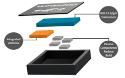
Another platform I saw at Embedded World was Silicon Labs’ WFM200 Wi-Fi SIP (Fig. 3). This SIP targets the Internet of Things (IoT) and combines a secure microcontroller with a radio and built-in antenna. The 6.5- by 6.5-mm chip supports 802.11 b/g/n as well as external antennas. One advantage of the internal antenna is that the chip is pre-certified by the FCC, CE, IC, and in South Korea and Japan. This can significantly reduce system design costs and the related expertise.
3. Silicon Labs’ WFM200 Wi-Fi SIP includes an integrated antenna.
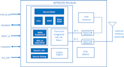
The WFM200 incorporates a variety of security-related features including secure boot, secure debugging, AES and PKE hardware accelerators, and a true random number generator (TRNG) (Fig. 4). There’s wireless support for packet traffic arbitration (PTA) coexistence, and it has a link budget of 115 dBm at 1DSSS. The receive power is only 48.6 mA at 1.8 V, while transmit power requirement is a mere 128 mA.
4. Among the security features integrated into the WFM200 is secure boot and a true random number generator.
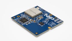
NXP’s IoT-on-a-Chip (Fig. 5) blends its i.MX family with Wi-Fi and Bluetooth connectivity plus 512 kB of SRAM and 2 MB of SST-eMRAM into a 14- by 14-mm FBGA. The latter is via Samsung’s foundry support for MRAM.
5. NXP’s IoT-on-a-Chip SIP combines an i.MX SoC with Wi-Fi and Bluetooth support. The chip is shown here in the upper left of NXP’s SOM board.
Designing with SIPs like the WFM200 and the OSD335X-SM can speed time to market. They also make it easier for designers to concentrate on their secret sauce while using the latest technology, without having to gain expertise in areas where SIP designers provide the solution.
