Google introduced a third generation of the machine learning chips installed in its data centers and increasingly available over its cloud. The company said that the new tensor processing unit, which is more commonly known as the TPU, is getting a major performance boost.
The company said at the Google I/O conference Tuesday that the new generation of chips would be packaged into machine learning supercomputers called pods that support more than a hundred thousand trillion floating-point operations per second – or 100 petaflops – over eight times the performance of the previous version of the pod.
In recent years, Google has become synonymous with using custom accelerators for artificial intelligence tasks like sorting images, training cars to drive themselves, and answering people when they ask questions. Other internet companies have started to follow its lead, as both Facebook and Amazon apparently kick the tires on custom chip design.
Google began building chips to get around the slowing pace of processor development. Manufacturing chips is growing so complex that companies now take almost three years to release new generations of chips. When it was first introduced in 2016, Google estimated that its custom TPU was seven years ahead of general-purpose processors for machine learning.
The project has taken shape as Google weaves more artificial intelligence into its services, a fact highlighted by Google chief executive Sundar Pichai and his lieutenants. John Krafcik, chief executive officer of Waymo, said Alphabet’s driverless car division uses Google’s TensorFlow software and TPU hardware to train algorithms that eliminate sensor noise caused by snowy streets.
Google’s bet on artificial intelligence is also reflected in the decision to rebrand its entire research division as Google AI. On Tuesday, the company said that more than 500 million smartphones and other devices use Assistant, which has been updated to understand more complex questions. Google also uses its machine learning smarts to sort through the electronic health records and automatically complete sentences in emails.
The firm’s first machine learning chip could only perform inference, making conclusions based on the algorithm’s training with millions of images, hours of voice recordings, or encyclopedias of text. That processor supports 92 teraops. The second generation of the TPU was introduced last year and handles both training and inference.
Google’s project has touched off major investments in the chip industry, including a secretive startup founded by former Google chip designers, with plans for an accelerator that handles 400 trillion operations per second. Dozens of companies are now fighting over the machine learning chip market dominated by Nvidia and hounded by the likes of Intel and AMD.
Last year, Google also introduced the concept of the pod, which uses high-speed interconnects to network hundreds of custom chips. Jeff Dean, now head of Google’s artificial intelligence unit, said that every pod would contain 256 second-generation chips and handle 11.5 petaflops. They will become available over the cloud later in 2018.
The new chips will feed its rivalry with Nvidia, which it has been trading blows with in recent benchmarks. Nvidia’s new server system, which uses custom switches to combine 16 GPUs based on the Volta architecture, supports two petaflops. Inside, each Tesla graphics chip handles 120 teraflops, almost three times as many as Google’s second-generation TPU.
Google’s plan has always been to offer the custom hardware over its cloud, differentiating itself from Amazon and Microsoft. In February, it started offering customers access to circuit boards called Cloud TPUs, which are equipped with four chips that together support 180 teraflops. That translates to around 45 teraflops for each of the TPU chips.
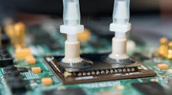
The third-generation chips generate so much heat while training and inferencing that Google had to introduce liquid cooling to keep them from catching fire. The hoses on the board carry water to each of the accelerators, which previously had heat whisked away by towering heat sinks. This is its first use of liquid cooling in data centers, Google said.
The architecture of the third-generation chips is still under wraps. Google would not say what was behind the performance boost of the new pod or when they would be available to cloud customers. One possibility, industry analysts say, is that the company has increased the number of chips that constitutes its current pod.
The new hardware shows that Google is not giving up on lowering the cost and increasing the availability of artificial intelligence. Whereas it could cost weeks and thousands of dollars to train image recognition models several years ago, Google can train them within a couple of hours, according to Stanford University’s DawnBench benchmark, costing less than $50 in some cases.
Google also put pressure on Nvidia to include custom tensor cores in its Volta architecture. Nvidia recently said that the latest Tesla GPU is four times faster at training image recognition algorithms on the ResNet-50 image database than chips based on Nvidia’s Pascal architecture. Google recently started to offer Nvidia’s latest chips over the cloud.

