Today’s high-speed FPGAs have a passing similarity to their older counterparts. However, large arrays of identical lookup tables (LUTs) and interconnect fabrics have given way to high-speed, networks-on-chip (NOCs) and specialized blocks targeting applications such as machine learning (ML). The solutions are almost more ASIC in nature, gaining the performance and efficiencies of that approach, but retaining the configurability of conventional FPGAs.
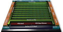
Achronix’s latest Speedster7t FPGAs incorporate all of these features to provide faster communication between ML blocks, storage, peripherals, and FPGA fabric (Fig. 1). It’s built on TSMC’s 7-nm FinFET process. Chips and development boards will be available in Q4.
1. The Speedster7t leverages TSMC’s 7-nm FinFET process.
The Speedster7t includes conventional FPGA blocks such as LUTs, DSP engines, and block memory sprinkled throughout the FPGA fabric that connects these components together. The challenge in large FPGAs is timing closure when information from one end of the fabric needs to get to the other side. This normally requires reducing the system clocking rate to meet design needs. DSP engines are one way to reduce connectivity requirements while providing a more efficient implementation, but this is on a small scale.
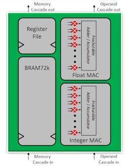
The machine-learning processor (MLP) blocks are significantly larger than a DSP block (Fig. 2). It would take multiple DSP engines to make up the integer or floating-point MACs in the MLP. The MLP also incorporates a register file and 72 kb of block RAM (BRAM). The MLP could be built up from conventional FPGA blocks; however, the resulting area would be two or more times larger and it would run slower. This is true when moving an FPGA design to an ASIC, but the cost is significant.
2. The Speedster7t machine-learning processor (MLP) block targets ML applications.
The MLP retains the configurability of an FPGA with its surrounding components and fabric while providing an efficient, cascadable ML accelerator. These larger MLP blocks can be combined to handle larger or multiple layers within an ML model. As with most ML accelerators, a single block will not handle an entire model, and even multiple blocks will have to be reused to manage very large ML models.
The MLP blocks are highly configurable themselves. The MACs can handle FP16 and a non-standard FP24, as well as TensorFlow’s BFloat16 plus 12- and 16-bit block float formats. The integer MACs support int4, int8, and int16 formats. The floating-point and integer sections can operate in tandem, allowing for custom numeric operations such as accumulating integer results, often used to reduce the size of ML data, as a floating-point value. The MLP BRAM is for general storage, while the register file is typically used to deal with cascading and channelization for larger ML models.
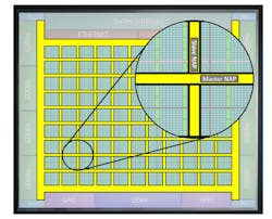
Though one might consider the large MLP blocks to be an enhancement along the lines of a super DSP block, the part of the Speedster7t that deviates from a conventional FPGA is the NOC (Fig. 3). The NOC consists of non-interconnected horizontal (master) and vertical (slave) communication highways. Near each intersection is a network access point (NAP) that allows the nearby FPGA fabric to link to the highways.
3. Achronix’s network-on-chip (NOC) implement uses non-overlapping communication highways with network access points (NAPs) near each intersection.
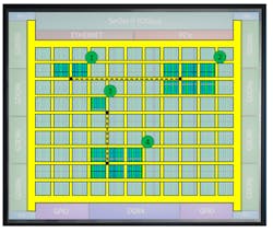
The highways are actually a bidirectional set of unidirectional lanes that connect one NAP to another (Fig. 4). Data enters a NAP and flows to the destination that will forward it in the desired direction. The highways overlap but don't connect to each other. To move data diagonally requires moving off via a NAP and onto another one.
4. The NOC allows for connections between blocks. However, the NOC operation is independent of the surrounding fabric, so no timing closure is required between connected blocks.
The lanes can operate in different modes depending on how data is handled. This includes transaction-oriented operations using an AXI-style interface, a packet-based interface for handling Ethernet-style packets, unpacketized data streams, and a NAP-to-NAP for handling communication from FPGA logic.
Each column or row has a bandwidth of 512 Gb/s. It’s a 256-bit-width channel running at 2 Gb/s. This number is key because the chips are designed to handle 400-Gb Ethernet. Total system bandwidth is 20 Tb/s.
The ports around the periphery of the chip include the Ethernet ports that can be configured to handle different speed interfaces up to 400 Gb/s. This also means that the system can distribute the 400 Gb/s quickly and efficiently to different sections of the FPGA along a column or row without having to worry about time closure on the system. That’s because the lanes operate independently of the fabric and other blocks like the MLP blocks.
The periphery of the NOC is also optimized for common operations. This lets the PCIe interface move data to and from the GDDR6 memory controllers. GDDR6 was chosen over on-chip HBM storage because of cost. The GDDR6 memory operates more slowly than HBM. It can be significantly larger while being faster than the DDR4 interface, which is also provided. DDR4 is at the bottom of the memory hierarchy, providing very large amounts of slower storage.
The PCIe Gen 5 and Ethernet interfaces are supported by the 112-Gb/s SERDES. The two PCIe ports support x16 and x8 interfaces.
The first chip out of the chute will be the 7t1500 with 692K 6LUT or 1522K 4LUT blocks. It has 2560 MLP blocks that deliver 211 TOPS with int4 data or 86 TOPS with int8 data. It will have thirty-two 112 Gb/s SERDES, eight GDDR6 interfaces, and a single DDR4 interface. The PCIe Gen 5 includes a x16 and x8 interface. It can handle four 4x 100-Gb/s Ethernet ports or two 8x 50-Gb/s ports. The top-end 7t6000 ups the 4LUT fabric to 5.72 million blocks and 134 MLP blocks.
The technology is also supported by Achronix’s Speedcore eFPGA IP. This allows the highways and MLP byways to be included in embedded applications. It also simplifies interfacing, since the ASIC can be connected to outer NAPs.
