OmniVision Unveils HDR Automotive Image Sensor, Wafer-Level Camera Module
Among the primary challenges facing engineers developing imaging sensors for automotive cameras is creating a high-dynamic-range (HDR) system that can detect and display LEDs without flicker. Achieving HDR involves the simultaneous capture of bright and dark areas in the same frame and the ability to combine multiple captures without sacrificing signal-to-noise ratio or introducing artifacts. Sensors with a low dynamic range typically deliver images that are largely under- or over-exposed, which means a loss of detail from these areas.
Another obstacle is LED flicker from headlights, road signs, and traffic signals, which occurs when a light source is being powered by a pulse-width-modulated (PWM) signal. LED lights may pulse several hundred times a second. At frequencies greater than 90 Hz, the light will usually appear to be constant to most human observers. A camera capturing the pulsed light source, however, may require a shorter exposure time than the “on” period of the PWM.
In response to what Pierre Cambou, Principal Analyst, Imaging from Yole Développement describes as automotive camera stakeholders “asking for higher performance, such as increased resolution, 140-dB HDR and top LED flicker mitigation (LFM),” OmniVision Technologies announced the OX03C10 ASIL-C automotive image sensor (Fig. 1). The company says it’s the world’s first to combine a 3.0-µm pixel size with an HDR of 140 dB and LFM performance.
The image sensor can deliver 1920- × 1280-pixel resolution at 60 frames per second (fps), enabling greater design flexibility and faster camera-view switching for drivers. In addition, according to OmniVision, the OX03C10 has the lowest power consumption of any LFM image sensor with 2.5-Mpixel resolution—25% lower than the nearest competitor—along with the industry’s smallest package size, enabling placement of cameras in even the tightest spaces.
In a separate announcement on the same day, the company also launched what it claims is the first automotive-grade, wafer-level camera. The 6.5- × 6.5-mm, 1-Mpixel module provides driver-monitoring-system (DMS) designers with flexibility on placement within the cabin.
Using a Deep Well
But first more on the OX03C10. Designed for high-end viewing applications in premium vehicles, it uses OmniVision’s Deep Well dual-conversion gain technology to provide “significantly lower motion artifacts than competing 140-dB HDR units,” said Kavitha Ramane, staff automotive product marketing manager at OmniVision.
“Deep Well” refers to full-well capacity. Full-well capacity is the largest charge a pixel can hold before saturation, which results in degradation of the signal. An image sensor’s dynamic range is typically defined as the full-well capacity divided by the camera noise and relates to the ability of a camera to record simultaneously very-low-light signals alongside bright signals.
Typically, HDR techniques require multiple exposures to achieve similar dynamic range when fast-moving objects are in the scene. This can lead to ghosting artifacts after combining the data into one HDR pixel value. This frequently happens with industry-standard dual-gang conversion HDR, which snaps two image shots in succession before conversion to create the image. OmniVision’s Deep Well pixel HDR achieves full-pixel images in one shot, generating a single readout charge with both low- and high-conversion gain to produce images without motion artifacts.
The sensor can be utilized for a wide range of automotive imaging applications, including rear-view cameras, e-mirrors, and surround-view systems. Its ability to provide LFM and HDR at high temperatures is important because applications like e-mirrors are often running continuously in extreme temperature conditions. E-mirrors enable unobstructed views (full cabin, rear, and side) as well as bright and clear rear vision with low-light sensitivity (e.g., they can better detect cyclists at night).
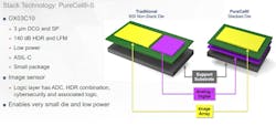
PureCel-S leverages OmniVision's stacked-die technology (Fig. 2), which separates the image-sensor array from the image-sensor processing pipeline. Stack technology is a two (or more) wafer solution that leads to smaller die size and higher-level integration in advanced camera features. For example, stacking allowed OmniVision to boost pixel and dark-current performance, resulting in a 20% improvement in the signal-to-noise ratio over the prior generation of its 2.5-Mpixel viewing sensors.
Another benefit of PureCel technology is the reduction of pixel crosstalk, which minimizes color crosstalk and color noise, improving color reproduction under low-light conditions. Another critical benefit is the angular response of the sensor; these sensors can provide higher signal response at a larger incident light angle, increasing the tolerance of camera systems to incident light angles. As a result, module design houses can use brighter lenses and build camera systems with thinner geometries.
The new OX03C10 image sensor is planned to be AEC-Q100 Grade 2 certified, and is available in both a-CSP and a-BGA packages.
Driver Monitoring
OmniVision claims its OVM9284 CameraCubeChip module is the world’s first automotive-grade, wafer-level camera. The 1-Mpixel module, measuring just 6.5 × 6.5 mm, provides driver-monitoring-system designers with flexibility on placement within the cabin; for instance, moving it from behind the steering wheel to the vertical A-pillar. In addition, the company noted that the module has the lowest power consumption among automotive camera modules—over 50% lower, they said, than the nearest competitor.
The integrated OVM9284 image sensor has a 3-µm pixel and a ¼-in. optical format, along with 1280 × 800 resolution. It’s built on the supplier’s OmniPixel3-GS (global-shutter) pixel architecture, which provides light-handling efficiency at the 940-nm wavelength. Thus, according to OmniVision, it results in high-quality driver images in near or total darkness. In a GS pixel-based image sensor, every pixel of the entire pixel array acquires the image during the same time period.
Unlike the OVM9284, “most existing DMS cameras use glass lenses, which are large and difficult to hide from drivers to avoid distraction, and are too expensive for most car models,” said Aaron Chiang, marketing director at OmniVision.
The OVM9284’s integration of OmniVision’s image sensor, signal processor, and wafer-level optics in a single compact package helps reduce the complexity of component acquisition and increases supply reliability while speeding development time. Furthermore, all CameraCubeChip modules are reflowable. This means they can be mounted to a PCB simultaneously with other components using automated surface-mount assembly equipment.
OVM9284 module samples are available now, and mass production is expected in Q4 of 2020.


