Bring True-Black and High-Fidelity Colors to Your Automotive TFT-LCD Display
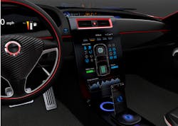
TFT-LCD displays are ubiquitous in modern cars, from instrument clusters (Fig. 1) to center-stacked touchscreens, rear-seat entertainment, and more. With displays playing an increasingly critical role in helping the driver navigate the road, their ability to accurately report information is critical for the safety of car occupants. Concurrently, rear-seat entertainment displays require high-quality images that don’t diminish the movie’s intended dramatic effects.
While the size and resolution of automotive displays have grown, their electronics have become more complex yet limited in both PCB size and cost. Many examples of increasing complexity are found in the array of power rails that bias the TFT-LCD (thin-film transistor liquid-crystal display) panel, the multiple voltage references for gamma correction, and the backlight power.
One shortcoming of traditional LCD displays has been the use of edge-lit backlights. Since the backlight LEDs are located along the edges of the panel, the LEDs can’t be completely turned off because pulse-width modulation (PWM) is set globally. This will make the display not truly black, but rather dark gray.
New LCD displays solve the problem by reengineering the backlight, from edge-lit to full-array LEDs (Fig. 2). Now the LEDs are uniformly distributed along the panel surface and each LED, or a small zone comprised of a few LEDs (one to four), can be individually controlled from full luminosity to full darkness. With local dimming, deeper blacks and more impressive contrast in the picture are obtained. In turn, they consume large amounts of power, requiring careful power-management implementations that maximize the LED driver’s efficiency in conjunction with powerful regulated power sources.
This article explores how a novel local dimming LED driver IC provides a high-contrast and high-dimming ratio, high current, high accuracy, low EMI, and a small solution size. A gamma buffer IC delivers 16 voltage references with 10-bit resolution, providing the least amount of gamma variation from panel to panel with low offset error at low cost. A complete TFT bias IC includes a current-mode boost converter, two push-pull charge-pump drivers, and a VCOM buffer driving the LCD backplane. Finally, a slew of standby, low-noise and POL voltage regulators provide the necessary high-voltage and low-voltage rails for a complete TFT-LCD display system solution.
TFT-LCD Display System
The standard display used in automotive systems is the active-matrix color TFT-LCD, which has become ubiquitous due to its high brightness, high resolution, reasonable cost, and demonstrated reliability in the challenging automotive environment. Liquid crystals have the ability to change their transmissivity with applied voltage. Each sub-pixel in an active-matrix TFT-LCD display receives its bias voltage (which sets its transmissivity) through a TFT transistor that acts as a switch. A pixel is made up of three sub-pixels, one for each of the primary colors: red, green, and blue.
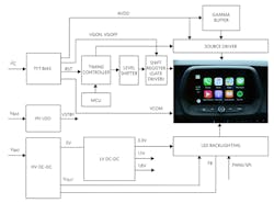
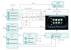
Figure 3 shows the main elements of the TFT-LCD display. The local dimming driver IC (LED BACKLIGHT) drives the backlight LEDs. The TFT BIAS powers the source and gate drivers and the gamma buffer; all of the power sequencing is driven by a microcontroller. A number of ancillary voltage regulators (HL/LV LDOs, HV/LV DC-DC) provide the necessary intermediate voltage rails.
Full-Array Backlight Example
As an example, a 12.3-in. instrument cluster display backlight panel is populated with a matrix of 256 LEDs. By dividing the 256 LEDs into 64 four-LED zones, the local dimming can be accomplished with only four 16-channel LED driver ICs. A 2s2p configuration of four LEDs in a zone assures string continuity even if one diode in each parallel element is open. Each diode has a maximum drop of 3.5 V and a mismatch between diodes of ±50 mV.
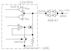
One of 16 channels is shown in Figure 4. The MOSFET-op-amp-resistor ensemble is the current sink that powers the 2s2p LED string, which can be dimmed with a switch via the op amp (OA) or shutoff. Two comparators provide overvoltage (VTHH) and short-to-ground protection (VTHL). The minimum channel output voltage VOUT (OUT16 in Fig. 4) is 0.8 V.
Each IC must operate under different conditions, including dissipating the power associated with 16 channels operating all at once. As an example, the IC has a junction-to-ambient thermal resitance (R) of 29°C/W with TA = +85°C. VDD must be set as low as possible and accommodate a ±50-mV mismatch between diodes. In a worst case, the 2s mismatch will be 100 mV.
The worse-case scenario for power dissipation is if one single 2s2p diode string develops a 7-V drop while the other 15 develop 6.9 V. If the dc-dc output is set to 7.9 V, then VOUT will be at 0.9 V (0.1 V above VOUT(MIN) = 0.8 V) and all the other 15 channels will be at 1 V. Accordingly, the worst-case power dissipation is:
P = (15 x 1 + 0.9) × 60 mA = 0.954 W
The IC junction temperature is well below our 150°C limit:
TJ = TA + R × P = 85 + 29 × 0.954 = 112.7°C
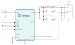
A feedback output pin (FB in Fig. 5) is necessary to control the external dc-dc converter so that voltage headroom can be optimized, and the overall system power dissipation reduced.
Integrated Backlight Driver Solution
As an example, the MAX21610 is a 16-channel modular backlight driver for use with automotive displays (Fig. 5, again). The integrated current outputs can sink up to a 100-mA LED current, depending on the ambient temperature. Device power comes from an external 3.3- or 5-V supply, while the LED current-sink outputs can operate up to 17 V. The global LED current for all strings is set through a serial peripheral interface (SPI), with individual PWM settings for each of the channels. Up to 10 devices can also be daisy-chained to reduce connection complexity. The IC comes in a 5- × 5-mm, 32-pin TQFN package and operates in the −40 to +125°C temperature range.
When mounted on a four-layer board, the junction-to-ambient thermal resistance is 29°C/W, enabling power dissipation in excess of 2 W. A 15-bit dimming ratio allows for up to 32,768 PWM dimmings steps at 200 Hz, which achieves the high-dynamic-range (HDR) display specification. Other features include open and short LED string detection and protection, overvoltage protection, thermal warning, and thermal shutdown. Spread spectrum and channel phase-shifting minimize EMI, while a 1% current-setting accuracy yields high color fidelity. Local dimming increases display contrast by making the black look deeper.
High Current DC-DC Converter
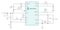
The dc-dc converter in Figure 5 can be implemented with MAX20006, a small, synchronous, automotive buck converter device with integrated high- and low-side MOSFETs (Fig. 6). The device can deliver up to 6 A with input voltages (SUPSW, SUP) from 3.5 to 36 V, while using only 25-μA quiescent current at no load. The state of the output voltage can be monitored by observing the active-low RESET signal. The device is able to operate in dropout by running at 98% duty cycle, suiting it for automotive applications. The IC is housed in a 3.5- × 3.75-mm, 17-pin FC2QFN package.
High-Power Buck-Boost Controller
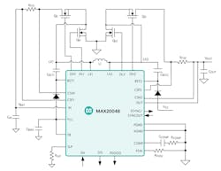
With the car battery power varying from less than 6 V (warm crank) to 16 V, the best configuration for delivery of intermediate voltages and high power is the buck-boost controller (e.g., the MAX20048 in Fig. 7). Here, only one inductor is utilized, versus a buck + boost that need two inductors. Housed in a 4- × 4-mm, 24-pin TQFN-EP SW package, it offers high-frequency operation of up to 2.2 MHz.
The device has synchonous rectification and an IQ of 55 µA; its output is adjustable from 4 to 25 V or is a fixed 5 V. It’s pin-selectable spread spectrum improves EMI performance and sync-in and sync-out pins allow for dual-phase operation when using multiple devices. Both the enable and input pin can support 40-V operation. In addition, its VIN(MIN) of 2 V after startup handles severe cold-crank operation. The IC operates from −40 to 125°C ambient and 150°C junction.
Standby Voltage
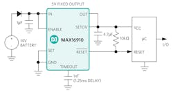
A standby-voltage regulator connects directly to the battery and has ultra-low quiescent current and wide input voltage operation. One example is the MAX16910 linear regulator, which targets automotive and battery-operated systems (Fig. 8). The device operates from a 3.5- to 30-V input voltage, delivers up to 200 mA of load current, and consumes 20 μA of quiescent current at no load. A 10-kΩ resistor between SETOV and OUT is recommended if line transients are expected to be faster than 0.03 V/μs. The device comes in a thermally enhanced, 3- × 3-mm, 8-pin TDFN package as well as a 5- × 4-mm, 8-pin SO package.
Gamma Buffer
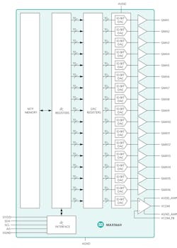
While backlight local dimming is necessary a for true-black display, gamma correction includes the full range of colors perceived by the human eye. Gamma correction of a digitally encoded image consists of allocating the available bandwidth according to the nonlinear perception of light and color by the human eye. To address this, the MAX9669 outputs 16 voltage references for gamma correction in TFT-LCDs and one voltage reference for VCOM (Fig. 9). Each gamma reference voltage has its own 10-bit digital-to-analog converter (DAC) and buffer to ensure a stable voltage. The VCOM reference voltage has its own 10-bit DAC and an amplifier to ensure a stable voltage when critical levels and patterns are displayed.
The IC incorporates integrated multiple time-programmable (MTP) memory to store gamma and VCOM values on the chip, eliminating the need for external EEPROM. It supports up to 100 write operations to the on-chip nonvolatile memory. The gamma outputs can drive 200-mA peak transient current and settle within 1 μs. The VCOM output provides 600 mA peak transient current and settles within 1μs. The analog supply voltage ranges from 9 to 20 V, and the digital supply voltage ranges from 2.7 to 3.6 V. Gamma values and the VCOM value are programmed into registers through the I2C interface. The IC is housed in a 5- × 5-mm, 28-pin TQFN package.
TFT Bias
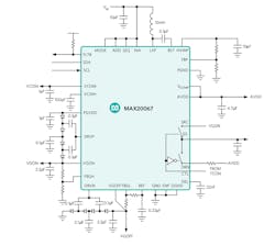
The TFT bias provides the several voltage rails needed by the LCD display. As an example, the MAX20067 three-channel display bias IC targeted at automotive applications includes a current-mode boost converter (HVINP) and two push-pull charge-pump drivers (VGON and VGOFF) (Fig. 10). The IC also includes a gate-shading push-pull level shifter that can be used to improve display uniformity (when needed), and a DAC and VCOM buffer. All blocks on the IC are usable in standalone mode or through the I2C interface. The MAX20067 comes in a 4- × 4-mm, 32-pin TQFN package.
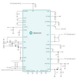
The four-channel MAX25221, another TFT bias chip, includes symmetrical positive AVDD and negative NAVDD supplies as well as VGON and VGOFF gate supplies. It has a VCOM buffer range below ground and a temperature measurement block that can measure the temperature optionally, allowing the VCOM output voltage to be adjusted depending on the measured temperature (Fig. 11). Programming is carried out using the built-in I2C interface, which can also be used to read back diagnostic information. A standalone mode is available after the device has been programmed. The IC is housed in a 5- × 5-mm, 32-pin TQFN package.
Low-Voltage, High-Efficiency POLs
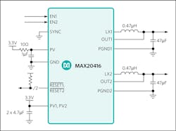
The backlight local dimming system requires several low-voltage, high-efficiency, point-of-load (POL) voltage regulators, such as the MAX20416 dual-output, low-voltage dc-dc converter (Fig. 12). The synchronous step-down converters operate from a 3.0- to 5.5-V input voltage range and provide a 0.8- to 3.8-V output voltage range up to 3 A. The buck converters achieve ±1.5% output error over line, load, and temperature range.
Low-Noise LDO
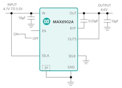
Another key component in automotive display solutions is the low-dropout regulator (LDO). Examples of these include the MAX8902A/MAX8902B low-noise linear regulators (Fig. 13). They deliver up to 500 mA of output current while reducing output noise to 16 μVRMS in a 100-kHz bandwidth. These regulators maintain their output voltage over a 1.7- to 5.5-V input range, requiring only 100 mV of input-to-output headroom at full load.
These LDOs maintain a 80-μA typical supply current, independent of the load current and dropout voltage. The regulator control circuitry includes a programmable soft-start circuit and short circuit, reverse current, and thermal-overload protection. The MAX8902A output voltage can be set to 1.5, 1.8, 2.0, 2.5, 3.0, 3.1, 3.3, 4.6, or 4.7 V using the SELA and SELB inputs. The MAX8902B output voltage is settable between 0.6 and 5.3V with an external resistor voltage-divider.
Conclusion
Automotive TFT-LCD displays require true-black and high-fidelity colors. The search for true, deep black in LCD displays is driving the transition from edge-lit to full-array LED backlights. In this article, we showed that a 12.3-in. LCD display backlight panel, populated with an array of 256 LEDs, can be effectively driven with just four daisy-chained LED driver ICs. Low IC and PCB thermal resistance assure maximum power delivery capability. A feedback loop connecting the LED driver ICs and a DC-DC voltage source that powers the LED strings assure proper voltage headroom to the four LED drivers’ output. This helps minimize the overall system power dissipation.
The backlight solution is complemented by a Gamma buffer that delivers 16 voltage references with 10-bit resolution. The TFT bias IC and a slew of standby, low-noise and POL voltage regulators provide the necessary high-voltage and low-voltage rails for a complete TFT-LCD display system solution that delivers true black and high-fidelity colors. Figure 14 shows an example of a state-of-the-art backlight local dimming system solution.
Szukang Hsien is the executive business manager for automotive display power and gesture solution, and Nazzareno (Reno) Rossetti is an analog and power management expert at Maxim Integrated.
