Meeting Code Execution and Data Performance Needs for Auto Apps
What you’ll learn:
- Key distinctions between NOR flash and NAND flash.
- How NOR flash and NAND flash can be deployed in automotive clusters and ADAS applications.
- The tradeoffs among flash memory density, performance, and cost.
The rapid evolution of cluster and advanced driver-assistance systems (ADAS) in automotive applications has led to corresponding changes—and advances—in memory technology. Rather than simply supporting a few dials and indicators, today’s clusters employ complex user interfaces that utilize a wide variety of memory-intensive technologies, including high-resolution graphics, live video from external cameras, GPS technology, streaming audio, nested menus, touch displays, and voice recognition.
ADAS systems place even greater strain on memory resources with the need for real-time video capture, object identification, movement prediction analysis, and environmental awareness such as reading road signs and assessing road conditions.
These demanding requirements on memory will only intensify over time. Operating systems like Linux continue to become more complex and expand in footprint. The display size and resolution are increasing and growing in popularity with autonomous-driving Level 2+ vehicles. Full graphics clusters are also appearing in high-end cars and will need to be cost-reduced before they can be adopted in more mass-market vehicles.
For these applications, a significant allocation of nonvolatile memory is required to store code, graphics, audio, and other types of data. Flash is commonly the non-volatile memory technology of choice, and developers can choose between NAND and NOR flash.
Primary considerations in memory technology selection include memory density, read/write performance, and cost. Ease of design is another consideration. Finally, because these are automotive systems, in which even minor data or code errors can result in injury or death, reliability is imperative.
Density, Performance, and Cost
A NAND cell is smaller than a NOR cell and has a lower cost per bit than NOR memory. As a result, higher densities are available in NAND flash than in NOR flash. Where NOR has generally held an advantage is in its ability to randomly access memory with short read times.
Traditional NAND flash can’t support bootstrap code execution across page boundaries, so systems storing code in NAND must transfer program code into RAM, where the system can then execute it. This has made NOR a more suitable choice for code-execution performance, particularly when Execute in Place (XiP) from NOR can be achieved.
However, recent advances in NAND technology that address inefficiencies related to code execution may help users overcome the cost challenge of designing in higher-density NOR flash. Serial flash, such as Macronix’s LybraFlash, addresses the code-execution issue by providing the user a NOR read experience that a normal NAND device can’t support. Such products enable continuous read, while memory-management features like bad-block management, wear leveling, and error-correcting code (ECC) achieve read compatibility and address data retention to approximate NOR flash.
Let’s go a bit deeper on the subject of continuous read. A normal NAND flash read operation is based on a “page” that MCUs can’t read continuously across, which causes a problem when the initial boot loader exceeds a page size. This gets resolved by adding the ability to read across pages.
The second issue related to continuous read is that NAND flash ships with approximately 98% good bits and experiences additional failures over the life of the memory. An MCU expects program memory to be contiguous, and these bad pages (blocks) result in fragmented code.
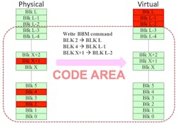
So continuous read mode, combined with bad-block management (BBM) and error correction code (ECC), allows an advanced serial NAND flash to execute code effectively and reliably. When initially programming or updating the device, an integrated BBM assures that bad blocks are avoided. A virtual map aligns all code blocks so that an MCU reading the memory will access code as contiguous blocks (Fig. 1).
ECC (see below) works hand in hand with BBM in maintaining the reliability of code memory; if an error or errors are detected, ECC usually can correct it. BBM in conjunction with MCU-based software then moves the code from the bad block to a good block and updates the virtual map, thus preserving the continuousness of code blocks.
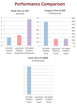
With continuous read mode, BBM, and ECC, advanced serial flash can reliably store both data and code. In effect, this advanced serial flash is able to provide or approximate the density, write performance, and cost effectiveness, along with the code execution capabilities of NOR (Fig. 2).
These features also result in a better boot key performance indicator (Boot KPI). Boot KPI is an important factor influencing the driver experience. Automotive clusters and ADAS need to boot quickly to avoid making drivers wait to start the car, turn on the radio, and get moving. As more features and even more code and graphics are added to these systems, developers need to continue to accelerate effective memory throughput to keep Boot KPI at acceptable levels.
Reliability and Ease of Design
Data integrity is essential in automotive applications. Although the chances are very small, memory bits can be flipped due to a variety of causes. ECC technology is an industry standard designed to identify and correct one or more bit errors, depending on the ECC algorithm in use. With ECC, systems are immune to certain types of data corruption, most notably single-bit errors. This enables such an advanced serial flash to provide the longevity required for automotive applications.
In advanced serial flash memories like LybraFlash, ECC is integrated into the memory (also known as “host-free” ECC). This simplifies system design as the memory manages its own ECC, transparently to the host MCU. Developers can also set an ECC bit-flip threshold to adjust the longevity of the overall memory. Integrated BBM also can simplify design by helping to offload bad-block management from the MCU as well.
One issue to consider when comparing memories with integrated ECC and BBM to those without these features is total cost of ownership (TCO). When computing TCO, developers need to account for any load on the host MCU in the form of drivers and middleware, as well as the impact on throughput and added complexity in overall system design. Factors like system responsiveness (i.e., boot time) may also come into play when they affect the user experience (i.e., delayed system startup or unacceptable latency).
For applications using this type of advanced serial flash for code execution, the combination of continuous reads across page boundaries, BBM, virtual mapping, wear leveling, and ECC assure that this flash will maintain high levels of reliability without requiring specialized programming from developers or burdening the host MCU. In addition, such serial flash memory is available in higher densities, making it possible to increase memory capacity while shrinking board footprint.
Summary
Memory-intensive systems like automotive clusters and ADAS require memory technologies that can deliver the performance and reliability required by these applications. The availability of high-density serial NAND memory enables these systems to store both code and data in a single memory device at a lower system cost.
With the option to use either high reliability NAND flash or NOR flash, developers have greater flexibility in design. Together, these nonvolatile memory technologies enable developers to choose the optimal capabilities for their application: NOR if faster random access is needed or NAND for faster write performance.
Jim Yastic, is Senior Technical Marketing Manager at Macronix America.


