Download this article in .PDF format.
The amount of electronic content in passenger cars continues to grow rapidly, driven mainly by the integration of various advanced driving and safety features. The industry’s move towards fully autonomous vehicles promises to even further increase the number of these advanced features and thus electronic content. What’s more, these components are becoming increasingly complex. The frontier for sophisticated semiconductors is found in the chips needed to execute artificial intelligence algorithms that govern emerging self-driving capabilities.
It is critical that these safety-related devices adhere to the highest possible quality and reliability requirements. These requirements are formalized in the ISO 26262 standard that covers all aspects of safety and quality for both the hardware and software, from design through testing and in-field operation.
More specifically, test for both large and small automotive ICs comes with these general requirements:
• Ability to detect errors in real time that could affect the safe operation of the system
• Very high defect coverage for manufacturing test to get single-digit DPPB (defective parts per billion)
To manage the new quality and in-system test requirements, as well as the ever larger designs that stress the design tool infrastructure and in-house compute resources, leading automotive IC makers are quickly adopting scalable design-for-test (DFT) architectures.
So what does a scalable DFT architecture and flow for large automotive ICs look like? The requirements for a DFT architecture are different depending on whether the IC is used for passive operations like display, infotainment, e-mirror, or proximity warning, or for more active operations like automatic-braking or smart-cruise.
It is essential that semiconductor companies deploy an automotive DFT architecture that it is scalable. It should support both the smaller sensor devices, right up to and including large AI devices used for processing the huge amount of data created in an autonomous vehicle environment. Mentor’s Tessent solutions are equally suited and relevant across this range of design types, ensuring that automotive semiconductor companies can invest in one scalable solution. Mentor has worked with a number of semiconductor companies making automotive ICs to build scalable DFT architectures.
Ensuring system reliability with in-line self-test
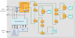
One approach to ensuring the reliability of a vehicle’s electronics is to perform periodic testing during functional operation. Designers can implement an architecture to provide system-level low latency access to all on-chip test resources for on-line test. In addition to these low latency access mechanisms, the entire test architecture is based on the IEEE 1687 (IJTAG) industry-standard architecture (Figure 1). An IEEE 1687-based network provides access to all of the test IP distributed throughout the design.
The test IP can consist of any IJTAG-compliant test IP. The hierarchical network of SIB (scan insertion bit) switches allows for versatile and efficient communication to the test IP. An IEEE 1149.1 TAP (test access port) provides external access to the IJTAG network and is primarily used within the manufacturing test environment. At the heart of the architecture shown in Figure 1 is Mentor’s Tessent MissionMode controller, which can take over the TAP signals and drive any test or diagnostic commands to any and all of the test IP in the IJTAG network.
The Tessent MissionMode controller can be configured to operate in two different modes: CPU access mode and direct memory access (DMA) mode.
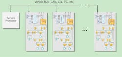
In CPU access mode, the controller supports parallel read and write operations to and from a CPU bus. The controller performs the parallel-to-serial and serial-to-parallel data conversion necessary to transport information between the CPU bus and the IJTAG network. This mode supports a module or system-level
communication architecture, as illustrated in Figure 2. A service and/or safety processor can access each Tessent MissionMode controller through the appropriate interface logic, and hence any on-chip test IP through any on-chip bus (e.g. APB) or any vehicle bus such as CAN (controller area network) or I2C (inter-integrated chip).
In the DMA mode, the controller reads command data preloaded in nonvolatile memory. Multiple test sequences can be stored and subsequently retrieved in any order and as many times as desired during system operation.
In addition to accessing the entire chip IJTAG network through the TAP, one or more in-system tests can also be configured to communicate directly to the component under test. This has the benefit of reducing communication latency, which can be critical for certain tests. One important example is nondestructive memory BIST. In this form of testing, the memory BIST controller tests the memory using a series of short sequences of transactions, often referred to as bursts. A burst will typically only last for a small number of clock cycles and target different memory locations each time. The entire memory is therefore tested over a large number of short memory BIST sessions. The approach is nondestructive because the memory locations that are modified by a burst are saved and restored during each burst by the memory BIST controller. Functional performance is not significantly affected because the bursts are only initiated when arbitration logic determines the memory is free. If memories are only to be tested at power-on, then the more traditional destructive memory BIST test can be used. In this case, latency is generally not an issue and a single Tessent MissionMode controller interfacing to the TAP is sufficient.
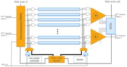
Logic BIST is another popular form of in-system test that can be accessed through the MissionMode controller. This test solution involves the on-chip generation of random patterns that are applied to scan chains. A recent improvement to this approach is a hybrid test solution that integrates both ATPG compression and logic BIST, as illustrated in Figure 3. Both of these solutions are typically required within automotive devices: ATPG compression for high-quality manufacturing test, and logic BIST for power-on, power-off, and on-line logic testing.
There are clear advantages to combining the two solutions. In particular, area overhead can be reduced as the two solutions use much of the same on-chip DFT resources. For example, they both make use of scan chains and related test clocks. The main difference between the two solutions lies in the on-chip logic feeding test data to the scan chains and processing the test response data coming out of the scan chains. There are also similarities in this logic so that the logic of the two solutions can be effectively combined to support both approaches.
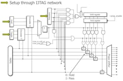
An important aspect of applying logic BIST periodically during functional operation is to limit power dissipation in order to minimize any effects on other parts of the system not under test. Reducing power during logic BIST operation can be achieved by minimizing toggle activity during loading and unloading of the random patterns and responses. The architecture shown in Figure 4 provides the ability to reduce scan toggle activity by periodically replacing random data bits with constant values. The architecture enables any arbitrary toggle rate to be programmed in the field. Toggle rates can be decreased while maintaining test coverage with some increase in pattern count.
Achieving very low DPPB with defect-oriented test
The widely used methodology for testing digital circuits is to add scan-test structures to the design and then deliver test patterns through these structures that reveal defects when the chip responses are observed. The approach has been in use for decades and is based on modeling circuit defects to a level of abstraction that enables a computationally efficient test-pattern generation process. The simple stuck-at fault model, which models circuit defects as logic nets stuck at either a 0 or 1 value, was initially used. More complex fault models were added over the years to account for new defect types that appeared as the industry transitioned to new technology nodes. Among the more recently adopted fault models were the transition, bridging, open, and small-delay faults.
However, with the move to smaller geometries these fault models and associated test patterns are becoming less and less effective at ensuring desired quality levels. The main problem is that all of these existing fault models only consider faults on cell inputs and outputs and only some defects on interconnect lines between these cells. In other words, only faults abstracted to the netlist level are explicitly considered.
It was shown in larger technology nodes (< 90 nm) that more defects occur within the cell structures. For the more advanced technology nodes and associated fabrication technologies, some estimates put the number of defects found within cells to represent almost half of all circuit defects. Various types of interconnect defects are becoming prevalent as well. Thousands of patterns are typically produced during the normal ATPG process. As a result, although traditional fault models do not target cell-internal and various cell-external defects explicitly, many of these defects end up being detected by chance. However, when considering millions of gates in a design and the need for very low DPPB levels, it is not effective to rely on luck to detect all potential defects. The more advanced Cell-aware Test (CAT) methodology directly targets physical defects internal to each cell, and the layout-aware bridge extraction methodology targets specific bridge defects on the interconnect between the cells.
Leveraging the proven layout-based design and library cell together with advanced critical area analysis (CAA) of the defect locations, the generation of manufacturing test patterns that effectively target defects at the transistor level inside cells, between adjacent cells, and in the interconnect based on critical area can be achieved. Published manufacturing test results demonstrate that these pattern types uniquely detect defects.
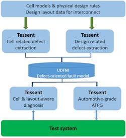
This technology is a two-step process to generate defect-oriented patterns targeting the automotive-grade quality requirements, illustrated in Figure 5. The first step is a characterization process to create accurate models for both cell-internal and design-related defects based on layout, design for manufacturability (DFM) rules, and CAA. The output is a user-defined fault model (UDFM) that describes the defects for both pattern generation and failure diagnosis. The second step is to create the patterns based on the generated defect models (UDFM). The defect coverage improvements may eliminate the need for other costly procedures such as system-level test and performance margining.
Analog fault simulation for high-quality mixed-signal circuit test
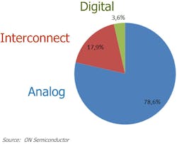
Cell-aware test, layout-aware test, and other advanced digital test solutions are going a long way in improving device quality. It turns out, however, that the majority of field failures in automotive devices now occur within the mixed-signal portion of the chip, as shown in Figure 6. This is not that surprising as the successful elimination of most digital defects means that any remaining defects will likely be mixed-signal in nature. These defects, albeit often small in number, cannot be tolerated in safety-critical automotive applications. Solutions are therefore needed to address this testing shortfall.
A basic prerequisite to automating the generation of analog tests is an automated means of measuring the fault coverage achieved by any test. Although fault simulation for digital circuitry has been commercially available for almost 30 years, analog fault simulation has only until very recently been discussed in academic papers and conferences. Being first to market with its commercial solution for analog fault simulation, Mentor offers a mature product that continues to be enhanced with new features.
The basic approach is to measure the coverage of opens and shorts and related parametric variations within a transistor-level netlist. Coverage of a given defect is determined by evaluating a change in the circuit response in the presence of the defect through analog simulation. What makes this approach now practical is the use of a number of significant speed-up techniques to reduce the analog simulation time by several orders of magnitude over simulating each defect one at a time on the flat netlist. These techniques include such things as likelihood-weighted random sampling to ensure most time is spent simulating the most likely defects, and mixed-model simulation where the highest-level model or netlist is used for each sub-circuit instance that does not contain the defect being simulated. This new automation enables a number of analog test related capabilities. First, existing analog tests can be evaluated for their effectiveness. Tests that do not cover any additional defects can be eliminated to reduce test time and cost. The new defect coverage metric can also be used to guide the generation of efficient new tests.
Defect tolerance and FMEDA analysis
Mentor’s analog fault simulator, Tessent DefectSim, can also be used to measure a circuit’s ability to continue to operate within acceptable operational parameters in the presence of various defects. This defect tolerance analysis is very important in automotive applications as it directly relates to long-term reliability. In the most general case, it is assumed that functional logic is monitored by some safety mechanism such as ECC or BIST. The impact of a defect can then be classified as shown in Figure 7.
Defects in the q1 and q2 quadrants do not affect the correct functional operation of the circuit and thus do not adversely affect safety. Defects in the q3 quadrant do affect functional operation but are detected by the safety monitor which places the circuit into a safe state. Defects in the q4 quadrant also effect functional operation and are unfortunately not detected by the safety monitor. The q4 defects, therefore, result in an unsafe state. Defect tolerance is then calculated as 1 – q4 / (q1+q2+q3+q4).
Designers can also generate other FMEDA (Failure modes, effects, and diagnostic analysis) related hardware safety metrics defined within the ISO 26262 standard. Tessent DefectSim is able produce reports suitable to support FMEDA creation.
Conclusion
Meeting the quality and reliability requirements of ISO 26262 and other automotive electronics standards becomes more difficult as device sizes and complexities continue to grow. Both the digital and analog portions of the chip must be fully addressed. The introduction of automation into the analysis and insertion of functional safety is allowing more comprehensive safety solutions to be implemented and qualified. They utilize in-system BIST solutions, such as logic BIST and nondestructive memory BIST, together with more conventional functional-safety mechanisms. These advancements, along with the adoption of advanced test capabilities such as automotive-grade ATPG for manufacturing test, will not only improve the ability of semiconductor manufacturers to achieve necessary quality and reliability metrics but will also help to further differentiate their products by delivering embedded test capabilities that can be leveraged by their customers at the system level and in the field. In addition, the calculation and delivery of failure metrics is also quickly becoming a key deliverable towards meeting necessary system functional safety goals.
Bio

