The Multi-Switch Detection Interface: A Cure for Many BCM Ailments
Download this article in PDF format.
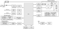
An automotive body control module (BCM) is an electronic control unit (ECU) that manages a wide range of vehicle comfort, convenience, and lighting functions, including the central locking system, power windows, chimes, closure sensors, interior and exterior lighting, wipers, and turn signals.
Figure 1 shows the functional blocks in a BCM. The primary function of the BCM is to monitor the status of discrete switches and analog sensors related to these functions and control high- and low-side switches, relays, and LED drivers. The BCM also exchanges information with other modules over a vehicle network: the Controller Area Bus (CAN) or Local Interface Network (LIN) protocols are both widely used.
Sponsored Resources:
- The multi-switch detection interface: integrated features for smaller, more efficient designs
- Video series: Multi-Switch Detection Interface (MSDI) for automotive and industrial applications
- Body control modules – invisible but fundamental for every car
- How to reduce the number of I/O pins with a switch matrix module
1. A BCM manages a wide range of comfort, convenience, and lighting functions. (Source: TI blog: “The multi-switch detection interface: integrated feature for smaller, more efficient designs,” Fig. 1)
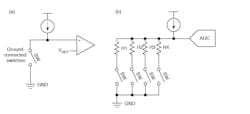
The number of switches and sensors varies from one vehicle to the other, but it can be 100 or more in a high-end implementation. There are two common types of switches in a vehicle (Fig. 2). A digital switch (Fig. 2a) only has two states, open and closed. Examples include the seat-belt engaged switch, rear-window defroster on/off, front and rear fog push button, the trunk switch, and the door-locking switch. The digital switch most commonly switches to ground, but switching to the battery voltage is also possible.
2. Digital (a) and resistive (b) switches are two common options in BCM applications. (Source: TI training: “Challenges in today’s Body Control Module (BCM) design”)
A resistive switch (Fig. 2b) has multiple states or positions. Each state connects a different resistor value to ground when selected. Examples include the ignition key switch, the taillight and headlight control switch, as well as the wiper control switch.
A microcontroller typically monitors the status of the various switches. Each type requires a different interface, but most MCUs feature general-purpose input/output ports (GPIOs) that can be configured to perform multiple functions. A digital switch can be sampled simply by a comparator, since it only has two states. An analog switch outputs a different voltage for each switch position, so the GPIO must connect to an analog-to-digital converter (ADC) to sample the value and determine the selected value.
Connecting a mechanical switch to an MCU involves a lot more than hooking up a wire. Two issues pop up: The low-voltage CMOS MCU input must be protected from external transients; and the switch contacts must be provided with a minimum wetting current that establishes a voltage to be measured, and prevents premature failure due to oxidation at the contacts.
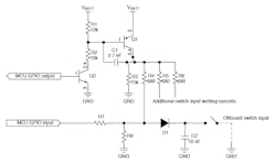
Let’s look at a simple switch-to-ground interface (Fig. 3). The traditional method of connecting an external ground-referenced switch uses numerous discrete components. For protection, capacitor C2 shunts ESD and transient energy, and diode D1 blocks high voltages. A GPIO output enables and disables the wetting circuit. A logic “high” output from the GPIO turns on the wetting current with the help of transistors Q1 and Q2; resistors R1, R2, and R3; and capacitor C1. Resistor R4 sets the wetting current at the switch. The voltage at the junction of R4 and R8 establishes the value at the GPIO input when the switch is open.
3. The interface for a mechanical switch requires multiple discrete components to protect the microcontroller and provide wetting current for the contacts. (Source: TI blog: “The multi-switch detection interface: integrated feature for smaller, more efficient designs,” Fig. 2)
In summary, each switch channel requires as many as five resistors, two capacitors, one diode, two FETs, and one unique GPIO connection.
Problems with the Discrete Approach
A discrete implementation such as shown in Fig. 3 poses several challenges for the designer:
High component count: The first issue is the high component count. For example, a BCM with 24 switch inputs requires a total of 78 resistors, 27 capacitors, 24 diodes, and six FETs. A large component count increases the size of the BCM, and pushes up the BOM and manufacturing costs.
High GPIO count: The 24-switch BCM also requires a total of 28 GPIO—one for each switch, plus four more to control the FET timing. This forces the use of a high-pin-count microcontroller, leading to increased cost and more complex PCB routing.
High power consumption: For fast switch response time, the microcontroller either needs to be active all of the time or be woken up periodically to ensure continuous switch monitoring.
A microcontroller typically draws milliamps of current. This might not be a problem, perhaps, when the vehicle is running and the alternator is charging the battery. However, when the ignition is off, automobile manufacturers require electronic modules to consume minimum quiescent current to prolong battery life. Keeping the BCM microcontroller alive to monitor switches may not be an option.
Variation in wetting current: The wetting current flowing through the switch in Fig. 3 depends on the battery voltage VBATT and resistor R4. Even during normal operation, VBATT can vary by several volts from its nominal value of 14 V due to transient load changes, and drop down to 6 V or less during cranking. Abnormal events such as load dumps and jump starts can cause much larger variations. The wetting current is proportional to the battery voltage. If the battery voltage changes by 20%, say, so does the wetting current.
The wetting current can also change with variations in resistive loading on the switch, especially if it's an analog switch with different resistances for different switch positions. Wetting-current variations complicate the system design. The effects can range from inconvenience to a system malfunction, especially if the BCM reads the wrong switch status.
Large ESD capacitor: The discrete design requires a large capacitor on each input to provide system-level ESD protection and prevent damage to other components on the PCB. A large capacitor on the input increases the time needed for the GPIO voltage to settle. This causes delay in the switch response time and forces the microcontroller to stay active longer, increasing the system power consumption.
Sharing of switch status: In some designs, a switch must be monitored by multiple microcontrollers for safety and redundancy reasons. When the same switch is connected to multiple microcontrollers, a blocking diode is typically needed to ensure the current flows only in the desired direction. These diodes increase cost and consume board space.
Design portability and reuse: With the large number of vehicle options available to consumers, creating portable and reusable designs across different platforms is a highly desirable goal. Each switch option (resistive switch, switch to ground, or switch to battery) requires a different discrete design, making it more difficult to create a uniform reference platform for multiple applications. This prolongs the design cycle and consumes more engineering resources.
The MSDI Device Provides an Integrated Solution
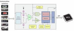
A multiple switch detection interface (MSDI) is a convenient way to take care of the issues discussed above. The MSDI integrates the discrete components for multiple channels into a single device (Fig. 4). It provides a common interface for multiple analog or digital switches and communicates their status back to an MCU via an industry-standard serial peripheral interface (SPI).
4. An MSDI device combines the interface components for many switch inputs into a single device. (Source: TI training: “How MSDI helps solve system-level challenges in BCM design”)
MSDI devices have adjustable wetting currents capable of sinking and sourcing currents for both battery- and ground-connected external switch inputs. These currents are internally monitored and controlled, so they remain consistent over a wide range of battery input voltages. MSDI switch inputs can also handle automotive load dump and reverse-battery voltages without the need for discrete blocking diodes and wetting-current components, saving additional board area and cost.
The TIC12400-Q1 is an MSDI device designed for the 12-V automotive environment. The device, which operates independently of the MCU, features a comparator to monitor digital switches, plus a 10-bit analog-to-digital converter (ADC) to monitor multi-position analog switches. Programmable detection thresholds for the ADC and the comparator allow the TIC12400-Q1 to support various switch topologies and system configurations.
The TIC12400-Q1 monitors up to 24 direct switch inputs. Ten inputs can monitor switches connected to either ground or battery. Each input can use one of six selectable wetting-current settings to support different application scenarios.
The integrated 10-bit, 0- to 6-V ADC measures the voltages on any input not set in comparator input mode, including any input threshold that requires special programming or any multi-threshold input. In addition, the ADC can directly monitor external analog signals.
The device can monitor all switch inputs while the MCU is in sleep mode. When action is needed, it can wake up the MCU with an interrupt, thus reducing power consumption of the system. The TIC12400-Q1 also offers integrated fault detection, ESD protection, and diagnostic functions for improved system robustness.
The TIC12400-Q1 supports two operational modes: continuous and polling mode. In continuous mode, wetting current is supplied continuously. In polling mode, TIC12400-Q1 turns on the wetting current to sample the input periodically, under control of a programmable timer. Poling mode significantly reduces the system power consumption.
For automotive applications without resistive multi-position switches, Texas Instruments also offers the TIC10024-Q1. This device has an identical feature set to the TIC12400-Q1, but without the ADC.
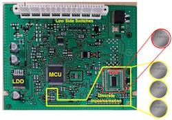
5. The MSDI-based solution consumes approximately 66% less board space than a discrete design. (Source: TI blog: “Body control modules—invisible but fundamental for every car”)
Figure 5 shows how the MSDI solution can save space versus a comparable discrete design. The underlying board is a BCM with a discrete switch interface. On it, we’ve superimposed, at a 1:1 scale, a snippet from the Automotive MSDI reference design—an example implementation using the TIC12400-Q1 device and required external circuitry. Both designs provide wetting current, reverse-blocking diodes, and ESD capacitors. With a two-layer board, the MSDI reference design measures 17.5 by 18.8 mm, one-third the size of the discrete solution.
TIC12400 Application Example: Resistive Switch
Using an MSDI certainly simplifies the hardware design and layout of a BCM switch interface. However, designing for the automotive environment requires the designer to pay close attention to a number of variables and tolerance stackups to produce a robust design.
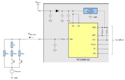
6. This application model is used to calculate allowable values for a three-position resistive switch. (Source: “TIC12400-Q1 24-Input Multiple Switch Detection Interface (MSDI)” PDF)
Let’s look at an example (Fig. 6) of the TIC12400-Q1 decoding the output of an analog resistor-coded switch with three states. When the switch changes state, the TIC12400-Q1 must correctly detect the state transition, store the information, and alert the MCU via an interrupt so that it can retrieve the data from the TIC12400-Q1’s status registers. The three states are:
State 1: Both switches open
State 2: SW1 open and SW2 closed
State 3: SW1 closed and SW2 open
Fig. 6 shows the switch specification. RDIRT represents the leakage across the switch in the open state; RSW1 and RSW2 are the two switch resistances; and R1 is the discrete resistor added in when switch 2 closes. The table shows the minimum and maximum values of these resistances. The TIC12400 sees an equivalent resistance RSW_EQU at the selected input pin INX.
Design example specifications. (Source: “TIC12400-Q1 24-Input Multiple Switch Detection Interface (MSDI)” PDF, p. 118)
To represent the automotive environment, we make the following assumptions: the battery voltage VBATT can vary between 9 and 16 V; and there is a potential ground shift of up ±1 V between the switch reference point and the ground reference of the TIC12400-Q1. The table shows the design specifications.
The design begins by calculating the equivalent resistance values at different switch states. After taking into account RDIRT and the 8% resistance tolerance of R1, each state yields a minimum, nominal, and maximum value for RSW_EQU.
When a switch closes, the current source in the TIC12400-Q1 sources a wetting current that flows through the switch. This current is nominally the set value IWETT, but is subject to variations over temperature and process, resulting in an actual current IWETT_ACT.
The nominal voltage at the INX pin is therefore:
VINX = RSW_EQU × IWETT_ACT
The ±1-V ground shift adds further uncertainty: The final measured value of VINX can be within a range of allowable values that all represent a valid switch configuration.
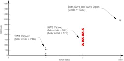
The three-position switch will have three sets of voltage bands (Fig. 7). These translate into three sets of valid ADC digital output codes, separated by code ranges that don’t correspond to a valid switch output. The designer can pick a code in the middle of each “invalid” range as the decision point for each switch position.
7. Each of the switch positions will result in a range of valid ADC codes separated by “no-go” bands. This example uses a nominal wetting current of 5 mA. (Source: “TIC12400-Q1 24-Input Multiple Switch Detection Interface (MSDI)” PDF, p. 120)
This example is covered in detail in the TIC12400 datasheet. There’s also a reference design, mentioned earlier—the MSDI reference design contains example implementations of a variety of high-voltage (HV) switch inputs using an MSDI device. The switch inputs satisfy a typical automotive requirement. They can withstand transients up to 40 V and reverse battery conditions down to –16 V.
The user guide gives examples of a TIC12400-Q1 or TIC10024-Q1 MSDI handling HV switch inputs for BCM, faceplate, and top-column-module (TCM) applications. In addition, the design utilizes a wide-VIN low-dropout (LDO) TPS7B6733-Q1 automotive regulator to create a fixed 3.3-V supply suitable for powering the BCM MCU.
Conclusion
As the number of comfort and convenience features in automobiles continues to increase, the BCM must interface with large numbers of switches in several different configurations, while simultaneously minimizing current consumption and keeping board small. A multi-switch detection interface (MSDI) device helps designers meet these requirements by bundling many standard interface requirements in a compact package.
Sponsored Resources:
- The multi-switch detection interface: integrated features for smaller, more efficient designs
- Video series: Multi-Switch Detection Interface (MSDI) for automotive and industrial applications
- Body control modules – invisible but fundamental for every car
- How to reduce the number of I/O pins with a switch matrix module

