Until recently, Schottky barrier diodes (SBDs) were commonly used in the reverse-connection protection circuits of advanced driver-assistance system (ADAS) camera modules. But due to the larger currents required by high-resolution cameras in advanced vehicle systems, SBDs are increasingly being replaced by compact MOSFETs that provide low on-resistance and less heat generation. For example, at a current and power consumption of 2.0 A and 0.6 W, respectively, conventional automotive MOSFETs can reduce mounting area by 30% over SBDs.
Adopting bottom-electrode MOSFETs that can provide the necessary heat dissipation while still supporting large currents in an even smaller form factor could make it possible to decrease mounting area by as much as 78% compared with conventional SBDs. But while bottom-electrode type MOSFETs can be miniaturized and still maintain high current, their use has been restricted by the fact that solder height can’t be verified after mounting by means of automated-optical-inspection (AOI) systems. Thus, it’s difficult to confirm mounting conditions.
To ensure the quality of automotive applications, a visual inspection is performed during assembly. AOI involves scanning boards with a camera to inspect for missing components or quality defects.
Leveraging “Wettable Flank”
According to ROHM, it’s the first in the industry to ensure the minimum solder height (130 μm) required for vehicle applications by utilizing its Wettable Flank formation technology. The technique makes a step cut into the leadframe on the side of bottom-electrode packages, such as QFN and DFN, before plating. This increases the solder joint surface between the package and substrate, improving solder wettability to allow for easy verification of solder condition after mounting.
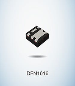
1. The growing number of safety and comfort systems in vehicles has made the space for these systems increasingly limited, thus driving demand for smaller components. The DFN1616 package measures just 1.6 × 1.6 mm. (Source: ROHM)
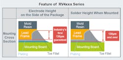
In previous attempts at using a step-cut solution, engineers found that burrs resulting from cutting into the leadframe occur more frequently as the height of the step cut increases. To overcome this limitation, ROHM developed a method that introduces a barrier layer on the entire surface of the leadframe to minimize the occurrence of burrs. This not only prevents solder defects during mounting, but it ensures a minimum solder height of 130 μm for DFN1616 (1.6 x 1.6 mm) packages (Fig. 1). The result is a consistent solder quality—even for compact products—enabling automatic inspection machines to easily verify solder conditions.
ROHM’s RV4xxx series of AEC-Q101-qualified MOSFETs takes advantage of this new package-processing technology (Fig. 2). The RV4xxx series contains two versions—RV4E031RP and RV4C020ZP—with the former’s on-resistance (at a VGS of 10 V) stated as 75 mΩ (typ.) and 105 mΩ (max). The parts have drain-source voltages of 30 V and 20 V and drain current of 3.1 A and 2.0 A, respectively.
2. According to ROHM, its new RV4xxx series is the first on the market to ensure a 130-μm electrode height on the side of the package. (Source: ROHM)
The RV4xxx series is now available in sample quantities; OEM quantities will begin in September.


