NXP Outfits Its First 5-nm Automotive SoC with Real-Time CPU Cores
As the larger automotive industry shifts its emphasis to software, NXP rolled out its first real-time, high- performance 5-nm SoC that can run more of this software safely, reliably, and securely.
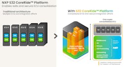
NXP said the S32N55 is the initial entry in its broader S32N family of “super-integration” processors, which sits at the top of the new S32 CoreRide central compute solution for software-defined vehicles (SDVs). These automotive-grade chips can unite up to “dozens” of different functions in the vehicle all at once, even in cases where they belong to different domains and require varying levels of functional safety. Merging all of these “mixed-criticality” systems in a safe, single system-on-chip (SoC) helps curb cost and complexity.
The S32N55 runs software that underpins these systems in several isolated execution environments inside the SoC. While it uses hypervisors and containers to keep them in separate software modules, it features full on-chip, hardware-enforced isolation to prevent workloads in one part of the processor from interrupting others. The CPU cores inside the SoC can also be configured in pairs so that they run in lockstep or separately to execute code independently.
NXP uses Arm’s Cortex-R CPU cores to carry out real-time processing in the SoC. It also brings a hardware security engine, in-vehicle networking, and a large amount of on-chip memory to the table.
Since it lacks higher-performance CPU and AI accelerator cores, NXP said the SoC is not designed in the same vein as NVIDIA’s Thor and Qualcomm’s “Flex” SoCs, which can run the software that underpins advanced driver-assistance systems (ADAS) and dashboard displays. It’s more of a “central controller” that can safely control the real-time domains in the vehicle, ranging from the powertrain that propels it down the road to the chassis that acts as the control unit for steering, braking, and more.
“The S32N55 processor is the central brain for real-time vehicle control,” said Ray Cornyn, NXP’s senior vice president and general manager of automotive processors.
A New Hardware Architecture Under the Hood?
As software assumes more responsibilities in cars, from battery management to ADAS and autonomous-driving (AD) systems, the underlying hardware used to control them is evolving, too.
The core building block in modern cars is the electronic control unit (ECU). In general, a microcontroller (MCU) sits at the heart of every ECU, and it often only has enough computing power to run a single task at a time.
In many cases, modern cars can have more than 100 separate ECUs, which are linked by huge masses of wiring that can add up in cost, space, and weight. Each unit tends to run on proprietary software developed by the specific supplier. That makes them largely inaccessible, even to automakers.
These control units are highly modular, which has been a boon for the automotive industry. But as their numbers rise, integrating them all together in the vehicle is becoming unsustainably complex, said NXP.
Today, automakers are replacing these boxes with a smaller number of large controllers—in some cases called “domain,” and in other cases, “zonal,” controllers—based on heterogeneous SoCs. Instead of using a separate MCU for every system in the vehicle, several functions can run in separate software modules on a single chip and communicate with each other through the same ECU. This architecture not only reduces the amount of hardware under the hood, but also cuts back on the bulky, heavy, and costly wiring inside.
Integrating software from several different domains in a single SoC has other merits. As a result, automakers can more regularly add new functions and features over time. For instance, the software inside the S32N55 could be upgraded to improve acceleration or steering around turns, enhance the stability of the vehicle in difficult road conditions, or help reduce the impact of a collision with another vehicle.
NXP is trying to stay on the front lines of this shift to SDVs with its S32N family of processors. The computing resources inside the S32N are dynamically partitioned so that it can meet the evolving requirements of the vehicle over time. Using its “software-defined” and “hardware-enforced” isolation, the company said the S32N55 can isolate everything from the real-time processing cores to the IO pins on the chip’s package.
The processor is also automotive grade. That means it has been painstakingly “qualified” to meet the most rigorous standards for functional safety (ISO 26262), security (ISO/SAE 21434), and reliability in vehicles.
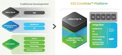
Despite all of the advances in hardware, software development in cars is still a non-trivial task. In general, it involves mixing and matching hardware with the building blocks that run on top of it in software, including the hypervisors, containers, operating systems, drivers, and the middleware that binds it all together. NXP is trying to cut through the complexity with its CoreRide platform, which is designed to decouple the underlying hardware from the software that customers load into it.
As part of the CoreRide solution, NXP is partnering with companies like Elektrobit, Green Hills Software, Wind River, and others to pre-integrate their software building blocks with its broader S32 family.
NXP said CoreRide gives automakers and Tier-1 suppliers the ability to develop applications separately from the underlying architecture of the vehicle and even the specific S32 processor in the vehicle.
Real-Time CPU Cores: Split Up or Locked Up for Safety?
The S32N55 itself contains four clusters of four split-lock Arm Cortex-R52 CPU cores running at 1.2 GHz for real-time computing. Because these cores can operate in either “split” or “lockstep” mode, they can carry out workloads with different degrees of functional safety, up to ASIL D. In lockstep mode, a pair of cores executes the exact same code and examines it for deviations that could indicate a fault condition.
CPU cores operating in lockstep can run safety-critical code with higher safety integrity. In split-mode, the cores execute independently, so they can be used for a wider range of tasks and applications.
While the S32N55 runs these workloads in different software modules, NXP said it specifically designed the hardware under the hood to keep them from interrupting each other—what it calls “freedom from interference.” It gives a separate runtime control for each ECU inside the SoC. In the event a fault occurs in one of the software modules, it’s prevented from impacting the other ECUs in the SoC.
The ECUs can also reset themselves without requiring the entire processor to restart itself. The S32N55 adds mechanisms to make sure every ECU has access to the networking bandwidth it needs.
A pair of lockstep Cortex-M7 cores is responsible for managing the functional safety of the system, while a second pair of Arm Cortex-M7 CPU cores manage all communications in and out of the processor.
Tightly coupled integrated memory and 48 MB of SRAM enable faster execution. The S32N55 can also be attached to LPDDR4X, LPDDR5, or LPDDR5X DRAM; LPDDR4X flash; and NAND or NOR flash memory for memory expansion. The memory is bolstered by error correction code (ECC) for more robust reliability. The SoC also adds cryptography on the data traveling to and from memory.
Communications and Connectivity
Ethernet is becoming the communications backbone in modern cars. As such, the S32N55 integrates a time-sensitive-networking (TSN) Gigabit Ethernet switch that runs from 10 Mb/s to 2.5 Gb/s.
The automotive-grade SoC features a wide range of connectivity interfaces, including 24x CAN FD, 2x CAN XL, 10x LIN, and 1x FlexRay interfaces. On top of that, NXP said it includes a subsystem that’s specifically designed to internally route the controller area network (CAN) buses without engaging the CPU at the heart of the SoC. The subsystem can use software to partition the CAN interfaces, so that different applications inside the SoC can share the same IO pins. Also in the mix is PCIe Gen 4 for chip-to-chip connectivity.
The hardware security engine acts as the root of trust (RoT) in the system and underpins secure boot.


