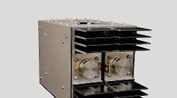
Cree and Kansai Electric Power Company (KEPCO) of Osaka, Japan, have demonstrated a silicon carbide (SiC) 3-phase inverter that delivers 110-kVA of output. This performance exceeds previously reported levels of power output for an inverter constructed using SiC power devices. Moreover, the output power produced by this inverter is nine times higher than the previous high of 12 kVA demonstrated by KEPCO and Cree in 2004. Because SiC-based inverters can dramatically lower conversion losses when compared with conventional inverters, this demonstration could pave the way for energy savings in a numerous applications.
The 110-kVA 3-phase inverter is based on SiC power devices fabricated by Cree. Kansai Electric took these SiC devices and constructed SiC modules, which it then used to construct the inverter. This project was part of a collaborative eight-year effort funded by Kansai Electric.
Inverters such as this one eventually could reduce power conversion losses by more than 50% compared to existing silicon (Si)-based inverters. On a global scale, the potential savings are great because inverters find use in a variety of applications requiring dc to ac conversion or adjustment of the operating frequency in variable speed motor drives. Among the applications that would benefit from the more-efficient inverters are heat pumps, industrial motors and electric vehicles. These inverters also could improve the efficiency of transferring power from batteries, wind mills and solar sources to the utility grid.
The SiC power device manufactured by Cree is a 4.5-kV, 100-A design called the SiC-commutated gate turn-off thyristor (SiCGT). This switch turns off or on in less than 2 µs, which is 10 times faster than the switching speed of an equivalently rated silicon gate turn-off thyristor (GTO). And unlike GTOs, this SiC device does not require a snubber circuit, reducing the inverter’s parts count and heat dissipation.
To develop the SiCGT, Cree had to overcome several obstacles, according to John Palmour, Cree’s executive vice president of advanced devices. There were the challenges of obtaining the desired values for blocking voltage, VF, and turn-on and turn-off speed. Improvement in one of these parameters may lead to degradation in the others, so numerous factors, including device design and epitaxial issues, had to be addressed to balance these conflicting design goals.
Another obstacle in developing the SiCGT was overcoming the crystalline defects called micropipes, which are inherent in SiC wafer manufacturing. This task becomes more difficult as the size of the die increases. Thus, a larger die is more to difficult to fabricate reliably (that is, with few defects and a reasonable yield per wafer). In this case, the inverter’s power handling requirements dictate that the SiCGT die measure 8 mm × 8 mm, which is particularly large for a SiC device. However, Cree leveraged its experience in fabricating SiC wafers to achieve sufficient crystal quality to produce the large die.
Kansai Electric’s SiCGT module was developed by packaging one SiCGT and one 6-mm × 6-mm SiC PiN diode in a metal package. The module can operate at higher temperatures (300°C) than conventional silicon modules (125°C) because it exploits a new high-temperature resin called Nanotec-resin KA100 for dielectric insulation. Six of these modules were used to construct the 110-kVA, 3-phase PWM inverter. This inverter operated at a switching frequency of 2 kHz.
“We are advancing SiC power device technology through a variety of improvements ranging from lower defect density crystal growth to improved epitaxial processes, device design and processing,” says Palmour. “While more development is required, these improvements are moving the technology closer to the point where a significant reduction in the need for new power plants and reduction in greenhouse gas emissions are possible.”
