This articles is part of the Power Management Series in the Power Management section of our Series Library.
Download this article as a .PDF eBook.
Power-management ICs provide management functions that support operation of the power distributed in the end-item electronic system. These ICs employ both analog and digital process for this supporting function.
Gate Driver ICs
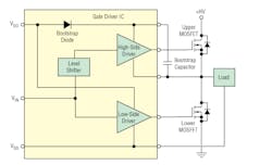
Gate driver ICs are power amplifiers to drive power MOSFETs in power-supply applications. Inputs to these gate driver ICs are typically logic levels from PWM ICs. Outputs can be single-ended or dual synchronous rectifier drive. MOSFETs require 1.0A to 2.0A drive to achieve switching efficiently at frequencies of hundreds of kilohertz. This drive is required on a pulsed basis to quickly charge and discharge the MOSFET gate capacitances. Figure 8-1 shows a basic gate driver IC for a power MOSFET.
8-1. Basic high-side and low-side drivers in a gate driver IC provides for synchronous rectifier connected power MOSFETs.
Gate drive requirements show that the Miller effect, produced by drain-source capacitance, is the predominant speed limitation when switching high voltages. A MOSFET responds instantaneously to changes in gate voltage and will begin to conduct when its gate threshold is reached and the gate-to-source voltage is 2.0V to 3.0V; it will be fully on at 7.0 V to 8.0 V.
Many manufacturers now provide logic level and low threshold voltage MOSFETs that require lower gate voltages to be fully turned on. Gate waveforms will show a porch at a point just above the threshold voltage that varies in duration depending on the amount of drive current available and this determines both the rise and fall times for the drain current.
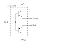
ZXGD3009E6/DY
8-3. IXYS’ IX2120 is a high-voltage IC that can drive high-speed MOSFETs and IGBTs that operate at up to +1200V.
High-voltage level-shift circuitry allows low-voltage logic signals to drive IGBTs in a high-side configuration operating up to 1200V. The IX2120B’s 1400V absolute maximum rating provides additional margin for high-voltage applications.
The IX2120B is manufactured on IXYS ICD’s advanced HVIC Silicon on Insulator (SOI) process, making the IX2120B extremely robust and virtually immune to negative transients and high dV/dt noise.
The inputs are 3.3V and 5V logic compatible. Internal undervoltage lockout circuitry for both the high-side and low-side outputs prevents the IX2120B from turning on the discrete power IGBTs until there is sufficient gate voltage. The output propagation delays are matched for use in high-frequency applications.
The IX2120B can drive power discrete MOSFETs and IGBTs in half-bridge, full-bridge, and 3-phase configurations. Typical applications include motor drives, high-voltage inverters, uninterrupted power supplies (UPS), and dc/dc converters. The IX2120B complements IXYS ICD’s extensive portfolio of high-voltage gate drivers, low-side gate drivers, and optically isolated gate drivers, and the full range of IXYS power semiconductors.
Features include:
- Floating channel for bootstrap operation to +600V with absolute maximum rating of +700V
- Outputs capable of sourcing and sinking 2A
- Gate drive supply range from 15V to 20V
- Enhanced robustness due to SOI process
- Tolerant to negative voltage transients: dV/dt immune
- 3.3V logic compatible
- Undervoltage lockout for both high-side and low-side outputs
- 28-pin SOIC package
Power-Factor Correction ICs
Most electronic systems use ac-dc switch-mode power converters that draw current from the powerline in a non-sinusoidal fashion that produces current and voltage distortions that can create problems with other equipment on the powerline.
Power factor describes the power relationships on an ac powerline. Current and voltage distortions occur with a reactive load, which has a real and a reactive power component. The vector sum of these two power components is the apparent power to the load. The phase angle between the real power and reactive power is the power factor angle. With a resistive load, the reactive power is zero and the apparent power equals the real power and the power factor is unity, or 100%. If the load is reactive, the power factor is lower (less than 100%).
For a nonlinear load with a distorted current waveform, the current consists of fundamental line frequency and various harmonics. These harmonic currents do not contribute directly to the useful power dissipated in the load, but rather add to the reactive power to create a higher value of apparent power. Total harmonic distortion, THD, is a common way of specifying and measuring the amount of distortion present on a waveform. Note that THD can be higher than 100%.
Most commonly used techniques for power-system electronics incorporate a power-factor correction (PFC) circuit ahead of the other electronics on the assembly. An example would be the PFC correction circuitry on the front end of an off-line ac-dc power converter. In addition, most systems that employ an active PFC utilize feedback circuitry along with switch-mode converters to synthesize input current waveforms consistent with high power factor.
The boost topology is the most popular PFC implementation. Almost all present-day boost PFC converters utilize a standard controller chip for the purposes of ease of design, reduced circuit complexity, and cost savings. These ICs greatly simplify the process of achieving a reliable high-performance circuit. In order for the converter to achieve power-factor correction over the entire range of input line voltages, the converter in the PFC circuit must be designed so that the output voltage is greater than the peak of the input line voltage.
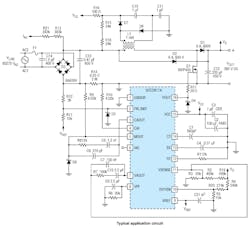
Figure 8-4 shows a typical application circuit for the UCC2818A-Q1 from Texas Instruments: a BiCMOS average current mode boost controller for high-power-factor high-efficiency pre-regulator power supplies. This active power-factor correction circuit pre-regulator programs the input current to follow the line voltage, forcing the converter to look like a resistive load to the line. A THD of less than 3% is possible with this circuit.
8-4. Texas Instruments’ UCC2818A-Q1 in a 250W PFC pre-regulator circuit.
For the circuit of Fig. 8-4, a switching frequency of 100 kHz, a ripple current of 875 mA, a maximum duty cycle of 0.688, and a minimum input voltage of 85 VRMS produces a boost inductor value of about 1 mH. The values used are at the peak of low line, where the inductor current and its ripple are at a maximum.
Power Over Ethernet (PoE) ICs
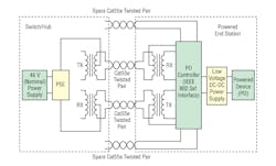
The IEEE 802.3af Standard states that all data terminal equipment (DTE) now has the option to receive power over existing cabling used for data transmission. The IEEE 802.3af Standard defines the requirements associated with providing and receiving power over the existing cabling. Figure 8-5 shows a typical Power-Over-Ethernet configuration. The power-sourcing equipment (PSE) provides the power on the cable and the powered device (PD) receives the power. As part of the IEEE 802.3af Standard, the interface between the PSE and PD is defined as it relates to the detection and classification protocol.
8-5. A Power-over-Ethernet system employs a power-source equipment (PSE) IC and a power-device (PD) IC and uses existing Ethernet cabling.
A PD draws power or requests power by participating in a PD detection algorithm. This algorithm requires the PSE to probe the link looking for a valid PD. The PSE probes the link by sending out a voltage between 2.8 V and 10 V across the power lines. A valid PD detects this voltage and places a resistance of between 23.75 kΩ and 26.25kΩ across the power lines. Naturally, the current varies depending on the input voltage. Upon detecting this current, the PSE concludes that a valid PD is connected at the end of the Ethernet cable and is requesting power.
If the PD is in a state in which it does not accept power, it is required to place a resistance above or below the values listed for a valid PD. On the lower end, a range between 12 kΩ and 23.75 kΩ signifies that the PD does not require power. On the higher end, the range is defined to be between 26.25 kΩ and 45 kΩ. Any resistance value less than 12 kΩ and greater than 45 kΩ is interpreted by the PSE as a non-valid PD detection signature.
After the detection phase, the PSE can optionally initiate a classification of the PD. The classification of a PD is used by the PSE to determine the maximum power required by the PD during normal operation. Five different levels of classification are defined by the IEEE 802.3af Standard.
Classification of the PD is optionally performed by the PSE only after a valid PD has been detected. To determine PD classification, the PSE increases the voltage across the power lines to between 15.5V and 20.5V. The amount of current drawn by the PD determines the classification.
Upon completion of the detection and optional classification phases, the PSE ramps its output voltage above 42V. Once the UVLO threshold has been reached, the internal FET is turned on. At this point, the PD begins to operate normally and it continues to operate normally as long as the input voltage remains above 30V. For most PDs, this input voltage is down-converted using an on board dc-to-dc converter to generate the required voltages.
Designers can still supply power in a limited fashion in some existing Ethernet installations via a mid-span bridge. But in that case, designers can’t implement power negotiations between a PD and PSE. This implies dedicated PoE Plus ports and relatively high duty-cycle power supplies in midspans.
Something else to watch out for is PDs that dynamically negotiate power requirements with the PSE via their Ethernet connection. This requires more code in the PD microcontroller and a greater understanding of dynamic power requirements on the part of the engineer writing that code.
The original 802.3af PoE standard offered a fairly straightforward way to supply loads with up to 13 W of usable power delivered at 48 V dc. But IEEE 802.3at PoE Plus ups usable power to something over 50 W, and introduces some wrinkles that designers and even IT managers must understand.
MAX5980A
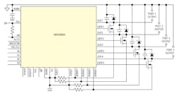
The MAX5980A from Maxim Integrated is a quad PSE power controller designed for use in IEEE 802.3at/af-compliant PSE (Fig. 8-6). This device provides PD discovery, classification, current limit, and load disconnect detections. The device supports both fully automatic operation and software programmability. The device also supports new 2-Event classification and Class 5 for detection and classification of high-power PDs. The device supports single-supply operation, provides up to 70W to each port (Class 5 enabled), and still provides high-capacitance detection for legacy PDs.
8-6. Maxim’s MAX5980A provides PD discovery, classification, current limit, and load-disconnect detections.
The device features an I2C-compatible, 3-wire serial interface, and is fully software configurable and program¬mable. The device provides instantaneous readout of port current and voltage through the I2C interface. The device provides input undervoltage lockout (UVLO), input over¬voltage lockout (OVLO), overtemperature protection, and output voltage slew-rate limit during startup.
The device provides four operating modes to suit differ¬ent system requirements. By default, auto mode allows the device to operate automatically at its default settings without any software. Semiautomatic mode automatically detects and classifies devices connected to the ports, but does not power a port until instructed to by software. Manual mode allows total software control of the device and is useful for system diagnostics. Shutdown mode terminates all activities and securely turns off power to the ports.
Switching between auto, semiautomatic, and manual mode does not interfere with the operation of an output port. When a port is set into shutdown mode, all port operations are immediately stopped and the port remains idle until shutdown mode is exited.
Voltage Reference ICs
Voltage reference provides an accurate, temperature-compensated voltage source for use in a variety of applications. These devices usually come in families of parts that provide specific accurate voltages. Some families can have up to six different values with output voltages ranging from 1.225V to 5.000V. Initial output voltage accuracy and temperature coefficient are two of the more important characteristics.
Voltage references are available with fixed and adjustable reference voltage outputs. Adjustable output is set by a resistor divider connected to a reference pin. These references are either shunt (two-terminal) or series (three-terminal) types.
The ideal voltage reference has a perfect initial accuracy and maintains its voltage output independent of changes in temperature, load current, and time. However, the ideal characteristics are virtually impossible to attain, so the designer must consider the following factors:
Shunt references (Fig. 8-7) are similar to zener diodes in operation because both require an external resistor that determines the maximum current that can be supplied to the load. The external resistor also sets the minimum biasing current to maintain regulation. Consider shunt references when the load is nearly constant and power-supply variations are minimal.
8-7. Shunt voltage reference.
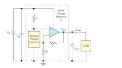
Series references (Fig. 8-8) do not require any external components and they should be considered when the load is variable and lower-voltage overhead is important. They are also more immune to the power-supply changes than shunt references.
8-8. Series voltage reference.
REF50xxA-Q1
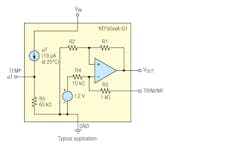
Texas Instruments’ REF50xxA-Q1 IC family is a low-noise, precision-bandgap voltage reference that is specifically designed for excellent initial voltage accuracy and drift. This family of voltage references features extremely low dropout voltage (Fig. 8-9). With the exception of the REF5020A-Q1 device, which has a minimum supply requirement of 2.7 V, these references can operate with a supply of 200 mV above the output voltage in an unloaded condition.
8-9. Texas Instruments’ REF50xxA-Q1 IC family is a low-noise, precision-bandgap voltage reference that is specifically designed for excellent initial voltage accuracy and drift.
These reference ICs provide a very accurate voltage output. If desired, you can adjust VOUT to reduce noise and shift the output voltage from the nominal value by configuring the trim and noise-reduction pin (TRIM/NR, pin 5). The TRIM/NR pin provides a ±15 mV adjustment of the device bandgap, which produces a ±15 mV change on the VOUT pin.
This family of reference ICs allows access to the bandgap through the TRIM/NR pin. Placing a capacitor from the TRIM/NR pin to GND in combination with the internal 1 kΩ resistor creates a low-pass filter that lowers the overall noise measured on the VOUT pin. A capacitance of 1 µF is suggested for a low-pass filter with a corner frequency of 14.5 Hz. Higher capacitance results in a lower cutoff frequency.
The REF50xxA-Q1 family has minimal drift error, which is defined as the change in output voltage over temperature. The drift is calculated using the box method. This reference family features a maximum drift coefficient of 8 ppm/°C for the standard-grade.
Temperature output pin (TEMP, pin 3) provides a temperature-dependent voltage output with approximately 60-kΩ source impedance. This pin indicates general chip temperature, accurate to approximately ±15°C. Although this pin is not generally suitable for accurate temperature measurements, it can be used to indicate temperature changes or for temperature compensation of analog circuitry. A temperature change of 30°C corresponds to an approximate 79 mV change in voltage at the TEMP pin.
VRM/VRD Power Management ICs
A voltage regulator module (VRM) is a buck converter that provides a microprocessor the appropriate supply voltage, converting +5 V or +12 V to a much lower voltage required by the CPU, allowing processors with different supply voltage to be mounted on the same motherboard.
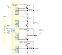
Fig. 8-10 is a typical VRM circuit.
8-10. VRM responds to the VID code from the microprocessor to provide the proper dc voltage.
Some voltage regulator modules are soldered onto the motherboard, while others are installed in an open slot designed especially to accept modular voltage regulators. Some processors, such as Intel Haswell CPUs, feature voltage-regulation components on the same package (or die) as the CPU, instead of having a VRM as part of the motherboard; such a design brings certain levels of simplification to complex voltage regulation involving numerous CPU supply voltages and dynamic powering up and down of various areas of a CPU. A voltage regulator integrated on-package or on-die is usually referred to as fully integrated voltage regulator (FIVR) or integrated voltage regulator (IVR).
Most modern CPUs require less than 1.5 V, as CPU designers tend to use smaller CPU core voltages; lower voltages help in reducing CPU power dissipation, which is often specified through thermal design power (TDP) that serves as the nominal value for designing CPU cooling systems.
Some voltage regulators provide a fixed supply voltage to the processor, but most of them sense the required supply voltage from the processor, essentially acting as a continuously variable adjustable regulator. In particular, VRMs that are soldered to the motherboard are supposed to do the sensing, according to the Intel specification.
Modern graphics processing units (GPUs) also use a VRM due to higher power and current requirements. These VRMs may generate a significant amount of heat and require heat sinks separate from the GPU.
The VRM concept was developed by Intel to guide the design of dc-dc converters that supply the required voltage and current to a Pentium microprocessor. The maximum voltage is determined by the five- to seven-bit VID (Voltage Identity) code provided to the VRM. The VID code connects the power supply controller to the corresponding pins on the microprocessor (Fig. 8-10). Therefore, the internal coding in the microprocessor controls the dc voltage applied to processor. VRM guidelines are intended for a special module, usually a small circuit board, that plugs into the computer system board and supplies power for the microprocessor.
A later version of guidelines are for a similar circuit called the Voltage Regulator-Down (VRD) developed by Intel to guide the design of a voltage regulator integrated onto the computer system motherboard with a single processor. These guidelines are based on the six-bit VID code.
At the present time and in the near future the VRM and VRD circuits must provide 60A to 100A for the Intel microprocessors. At this time, the only practical circuit that can provide those current levels is the multiphase configuration. Multiphase converters employ two or more identical, interleaved converters connected so that their output is a summation of the outputs of the cells.
Hot-Swap Controller ICs
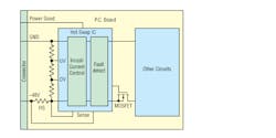
Often, equipment users want to replace a defective board without interfering with system operation. They can do this by removing the existing board and inserting a new board without turning off system power, a process called “hot-swap.” Figure 8-11 shows a typical hot-swap IC circuit. When inserting a plug-in module or p.c. card into a live chassis slot, the discharged supply bulk capacitance on the board can draw huge transient currents from the system supplies. Therefore, the hot-swap circuit must provide some form of inrush limiting, because these currents can reach peak magnitudes ranging up to several hundred amps, particularly in high-voltage systems. Such large transients can damage connector pins, p.c. board etch, and plug-in and supply components. In addition, current spikes can cause voltage droops on the power distribution bus, causing other boards in the system to reset. Therefore, a hot-swap control IC must provide startup current limiting, undervoltage, overvoltage, and current monitoring that prevents power supply failure.
8-11. Hot-swap control IC provides startup current-limiting, undervoltage, overvoltage, and current monitoring that prevents power-supply failure.
At a hardware level, the hot-swap operation requires a reliable bus isolation method and power management. With today’s power-hungry processors, careful power ramp up and ramp down is a must, both to prevent arcing on power pins and to minimize backplane voltage glitches.
Connectors employed in these systems must also allow safe and reliable hot-swap operation. One technique is to use staged pins on the backplane with different lengths. This allows events to occur in a time-sequenced manner as cards are inserted and removed. It enables the power ground and signal pins to be disconnected and then connected in an appropriate sequence that prevents glitches or arcing. After insertion, an enable signal informs the system to power up so that bus-connect and software initialization can begin.
One software sequence of the extraction-insertion process starts with an interrupt signal informing the operating system of the impending event. After the operating system shuts down the board’s functions, it signals the maintenance person or operator via an LED that it is okay to remove the board. After installing a new board, the operating system automatically configures the system software. This signaling method allows the operator to install or remove boards without the extra step of reconfiguring the system at the console.
PI2211
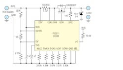
The PI2211 hot-swap controller and circuit breaker from Picor (now Vicor Power) ensures safe system operation during circuit card insertion by limiting the start-up or in-rush current to the load and eliminating the electrical disturbance or possible voltage sag imposed on a backplane power supply. During steady state operation, the PI2211 acts as a circuit breaker, disconnecting from the backplane power source if a overcurrent condition arises. The PI2211 uses an external N-channel MOSFET and employs the MOSFET’s transient thermal characteristics (supplied by the MOSFET supplier) to ensure operation within the MOSFET’s dynamic safe operating area (SOA).
In Fig. 8-12, the PI2211 limits the start-up current to a load, eliminating the electrical disturbance or possible voltage sag imposed on a backplane power supply. The PI2211 performs hot-swap protection during power-up or insertion and acts as a circuit breaker during steady state operation. The PI2211 performs these protection functions by controlling an external MOSFET and limiting the MOSFET junction temperature rise to a safe level, a key requirement for hot swap power managers expected to operate over wide dynamic conditions.
8-12. Picor’s PI2211 hot-swap controller and circuit breaker ensures safe system operation during circuit card insertion by limiting the start-up or in-rush.
Upon insertion, the PI2211 initiates a user programmable turn-on delay where the gate of the MOSFET is held “off,” providing input BUS de-bounce. The PI2211 then turns “on” the MOSFET pass element in a controlled manner, limiting the current to a pre-defined level based on the value of a user selected sense resistor. The PI2211 circuit breaker threshold protects against over-current by comparing the voltage drop across this sense resistor with a fixed internal reference voltage. Once the load voltage has reached its steady-state value, the Power-good pin is asserted “high” and the start-up current limit is disabled. Under Voltage (UV) and Over Voltage (OV) trip points (user settable) ensure operation within a defined operating range in addition to a Enable/Disable feature shared with the UV input.
With Power-good established, the load current is continuously monitored by the PI2211 with the MOSFET operating in the low-loss RDS(ON) region. In this steady state operation, the PI2211 now acts primarily as a circuit breaker. An over-current threshold is fixed to be twice the start-up current limit and sets an upper current boundary that determines when a gross fault has occurred. Exceeding this boundary will initiate the PI2211 Glitch-Catcher circuitry and assert the power good pin low. Glitch-Catcher prevents overvoltage events caused by the energy stored in the parasitic inductance of the input power path in response to a rapid interruption of the forward current during an overcurrent fault event. Acting as an active snubber, this circuitry mitigates the need for large external protection components by shunting the energy through the MOSFET to the low impedance load.
For the design example of Fig. 8-12, system requirements are:
- Nominal BUS voltage (VBUS) = 12V
- High BUS voltage where controller must be enabled (VBUSHIGH) = 12.5V
- Low BUS voltage where controller must be enabled (VBUSLOW) = 11.5V
- Maximum Operating Current (IMAX) = 10A
- Circuit Breaker Threshold (ICB) = 13A
- Hot-Swap Efficiency > 99%
- Schottky Diode is 40V, 1A; required to protect the SCR pin from negative voltage transients that can damage the controller. The 100Ω series resistor is used to limit current.
Supervisor ICs
Supervisory ICs ensure that the system-power supplies operate within specified voltage and time windows. In its most basic form, a supervisory IC compares a power supply voltage with a specific threshold. If the power source reaches that threshold, the supervisory IC generates a pulse that resets the system processor.
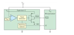
Figure 8-13 shows a simplified diagram of supervisor IC and its associated microprocessor. The voltage monitoring section of the supervisory IC includes a comparator and voltage reference as well as reset generator that can reset the associated microprocessor. Usually, supervisor ICs consist of a family of parts set for different thresholds, such as 1.5 V, 1.8 V, etc. There are also supervisor ICs that have adjustable thresholds. This supervisor IC has a watchdog timer that protects against an interruption in software execution. Usually, the watchdog timer is a restartable timer whose output changes state on timeout, resetting the system processor or generating an interrupt.
8-13. Supervisory IC ensures that the system power supplies operate within specified voltage and time windows.
Many systems require multiple supply voltages that can be monitored with multiple devices, but some of the supervisory ICs can monitor two or more voltages. Typically, the number of threshold voltages required in a system depends on the number of processor and peripheral power supplies.
The reset function of the supervisory IC may provide a power-on-reset (POR) to eliminate problems during power-up or a supply voltage sag. These problems can occur because of a slow-rising supply voltage, a supply voltage that exhibits noise or poor behavior during startup, or recovery from a sag. Typically, the reset circuit’s voltage tolerance should not exceed ±2.7% over temperature.
Many supervisory ICs include undervoltage and overvoltage comparators with programmable thresholds. Inputs for these comparators can implement a windowed reset that warns if a particular voltage is either too high or too low.
To ensure the continuity of processor memory contents and other critical functions if a supply voltage is lost, many of the older supervisory circuits are able to switch the memory’s power source to a backup battery.
MIC826
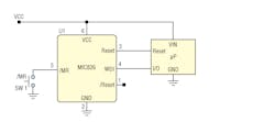
Micrel’s MIC826 is a low-current, ultra-small, voltage supervisor with manual reset input, watchdog timer, and active-high and active-low push-pull outputs (Fig. 8-14). This provides the designer with high integration while reducing solution size up to 70% compared to competing solutions. The IC also improves the accuracy of the power supply monitor by 1 to 2% over the -40°C to +125°C temperature range. This makes it an ideal solution for portable, as well as industrial and automotive applications.
8-14. Micrel’s MIC826 is a low-current, ultra-small voltage supervisor with manual reset input, watchdog timer, and active-high and active-low push-pull outputs.
It contains eight reset threshold options and is intended to monitor 1.8V to 5V power supplies. The IC features a ±0.5 percent voltage threshold accuracy at room temperature and ±1.5 percent voltage threshold accuracy over the -40°C to +125°C temperature range. The solution consumes a low 3.8µA of supply current for power supplies; lower than 3.6V and 4.8µA for solutions operating from a 5V power supply. The IC also features an industry standard reset timeout period of 140ms (min) and a watchdog time output period of 1.6s. The watchdog input can be left unconnected for applications that do not require watchdog monitoring.
The MIC826 consumes a quiescent current of only 3.8μA and is offered in a tiny, space-saving, 6-pin 1.6mm x 1.6mm Thin DFN package.
Load-Share Controller ICs
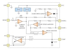
System integrators can improve system reliability with redundant, paralleled power supplies that share the load. Load-sharing distributes load currents equally among paralleled voltage-stabilized supplies. For the shared supplies to operate efficiently, the power system must ensure that no supply hogs the load current while other supplies are essentially idle. Also, the power system must be able to tolerate the failure of any one supply as long as there is sufficient current capacity from the remaining supplies. This requires the combination of power supplies to behave like one large power supply with equal stress on each of the units.
Individual load-shared supplies require an external controller, otherwise the supply with the highest output voltage will contribute most of the output current. Output impedance of typical power supplies is in the milliohm range so a small difference in output voltages can cause a relatively large difference in output currents. This might cause the supply providing the majority of load current to enter the current-limit mode, increasing its thermal stress, which would decrease system reliability. A load-shared system should have a common, low bandwidth share bus interconnecting all supplies. It should also have good load-sharing transient response and the ability to margin the system output voltage with a single control.
The UC3902 from Texas Instruments is a load share controller IC that balances the current drawn from independent, paralleled power supplies (Fig. 8-15). Load sharing is accomplished by adjusting each supply’s output current to a level proportional to the voltage on a share bus.
8-15. Texas Instruments’ UC3902 is a load-share controller IC that distributes load currents equally among paralleled voltage-stabilized supplies.
The master power supply, which is automatically designated as the supply that regulates to the highest voltage, drives the share bus with a voltage proportional to its output current. The UC3902 trims the output voltage of the other paralleled supplies so that they each support their share of the load current. Typically, each supply is designed for the same current level although that is not necessary for use with the UC3902. By appropriately scaling the current sense resistor, supplies with different output current capability can be paralleled with each supply providing the same percentage of their output current capability for a particular load.
Power Supply Management ICs
There are a variety of power-up profiles to satisfy the requirements of digital logic circuits including FPGAs, PLDs, DSPs and microprocessors. Certain applications require one supply to come up after another. Other applications require the potential difference between two power supplies must never exceed a specified voltage. This requirement applies during power-up and power-down as well as during steady-state operation.
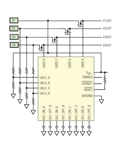
The Intersil ISL6123 is an integrated 4-channel controlled-on/controlled-off power-supply sequencer (Fig. 8-16) with supply monitoring, fault protection and a “sequence completed” signal (RESET).
8-16. Linear Technology’s LTC6123 is an integrated 4-channel controlled-on/controlled-off power-supply sequencer.
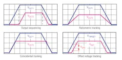
Figure 8-17.1. Timing diagram for output sequencing(top left)
Figure 8-17.2. Timing diagram for ratiometric tracking(top right)
Figure 8-17.3.Timing diagram for coincidental tracking(bottom left)
Figure 8-17.4.Timing diagram for offset voltage tracking(bottom right)
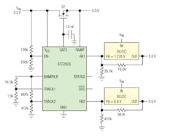
Another power-supply management function is tracking that ramps supplies outputs up and down together. In other applications it is desirable to have the supplies ramp up and down with fixed voltage offsets between them or to have them ramp up and down ratiometrically. Linear Technologies’ LTC2923 can provide power-supply tracking and sequencing. The associated supplies can be configured to ramp-up and ramp-down together or with voltage offsets, time delays or different ramp rates (Fig. 8-18).
8-18. Linear Technology’s LTC2923 sink/source tracking termination regulator.
Voltage margining is a means of verifying the robustness of a product by intentionally adjusting its supply voltages to their limits and then evaluating the product’s performance. This process evaluates the load circuit’s ability to tolerate changes in the power supply voltages that may occur over time and temperature. The testing is typically performed by forcing the power supply to ±5% of its nominal output voltage and then ensuring that the equipment still passes its final acceptance test.
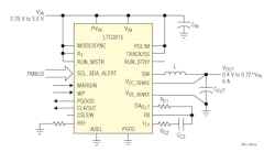
The LTC3815 from Linear Technology is a high-efficiency, 6A monolithic synchronous buck regulator using a phase lockable controlled on-time, current mode architecture (Fig. 8-19). Its I2C-based PMBus interface allows the output voltage to be margined using its internal 9-bit DAC that provides up to ±25% adjustment at 0.1%/bit resolution around the reference voltage set at the REF pin.
8-19. Linear Technology’s LTC3815 provides up to ±25% margining adjustment at 0.1%/bit resolution around the reference voltage.
The digital offset value is changed with a PMBus command. When a change in the reference is detected, the reference is ramped (0.1%/step) from its current value to the new value at a rate set by the capacitor value connected to the CSLEW pin, which provides a programmable slew rate of the VOUT transition. If desired, you can pre-loaded the LTC3815 with two additional offsets using PMBus commands. The reference offset can then be switched between any of these three register values with the 3-state MARGIN pin. When using the MARGIN pin, the latency of the VOUT transition is limited only by the chosen CSLEW capacitor and the loop bandwidth of the power supply. Changes to these registers are prevented by pulling the write protect (WP) pin high.
Intelligent Power-Switch ICs
Automotive body electronics modules routinely use intelligent power switches to control loads such as lamps, LEDs, solenoids, and motors. These switches replace mechanical relays to reduce mechanical noise, and shrink module size while increasing functionality.
Many years of development have produced today’s low-cost devices that are efficient, safe, flexible, reliable, robust, and fault-tolerant. Now, those same advances are being extended to intelligent power switches designed for the more demanding requirements of 24 V systems. Requirements of a solid-state switch for 24 V truck and bus systems must consider what we have already learned from the use of solid state switches in 12 V systems. Many of the requirements of 12 and 24 V systems are similar.
The primary requirement is low cost. Here, the entire system cost as well as the device cost is of interest. This includes the cost of thermal management, MCU overhead and pin count, PCB area for mounting and routing, additional circuitry needed for diagnostics and fault management, protection components such as capacitors needed to suppress voltage transients, etc. To minimize system costs associated with managing power, the latest devices have very low on-resistances to reduce power dissipation. Additionally, their SPI interface makes many control and diagnostic features possible and reduces MCU overhead and pin count. The SPI interface also greatly reduces routing complexity and saves PCB area.
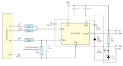
International Rectifier’s (now Infineon) AUIR33402S is a seven-terminal, high-side switch for a variable speed dc motor whose features simplify the design of the dc motor drive with a microcontroller. The MOSFET switches the power load proportionally to the input signal duty cycle at the same frequency and provides a current feedback on the IFBK pin. The over-current shutdown is programmable from 10A to 33A. Over-current and over-temperature latch OFF the power switch, providing a digital diagnostic status on the input pin. In sleep mode, the device consumes less than 10uA. Further integrated protections such as ESD, GND and Cboot disconnect protection guarantee safe operation in harsh conditions of the automotive environment.
The recommended connection with reverse battery protection in shown in Fig. 8-20.The basic circuit provides all the functionality to drive a motor up to 33A DC. Rlfbk sets both the level current shutdown and the current feedback reading scale.
8-20. Recommended circuit for International Rectifier’s AUIR33402S used as an intelligent power module to drive a motor.
DDR Memory Termination Supply ICs
DDR memories require terminal regulators, power supplies that minimize timing skew and power dissipation. The voltages involved in this termination process are VDDQ, VTT, and VREF. According to the JEDEC specification: VTT = 0.5 (VDDQ), VREF is a buffered reference voltage that also tracks 0.5(VDDQ) and VTT must track VREF with <40mV offset regardless of variations in voltage, temperature, and noise.
DDR memory systems employ Series Stub Termination Logic (SSTL) that improves signal integrity of the data transmission across the memory bus. This termination scheme is essential to prevent data error from signal reflections while transmitting at high frequencies encountered with DDR RAM. This termination configuration prevents data error from signal reflections while transmitting at the high frequencies associated with DDR memory. It involves the use of the termination regulator and termination resistors that regulate the voltage to 0.5(VDDQ).
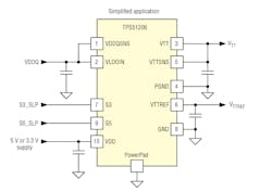
The TPS51206 from Texas Instruments (Fig. 8-21) is a sink/source tracking termination regulator specifically designed for low input voltage, low cost, and low external component count systems where space is a key application parameter. The TPS51206 integrates a high-performance, low-dropout (LDO) linear regulator (VTT) that has ultimate fast response to track ½ VDDQSNS within 40 mV at all conditions, and its current capability is 2 A for both sink and source directions.
8-21. Texas instruments’ TPS51206 DDR is a sink/source tracking termination regulator.
A 10-μF (or greater) ceramic capacitor(s) need to be attached close to the VTT terminal for stable operation; X5R or better grade is recommended. To achieve tight regulation with minimum effect of trace resistance, the remote sensing terminal, VTTSNS, should be connected to the positive terminal of the output capacitor(s) as a separate trace from the high current path from the VTT pin.
The TPS51206 has a dedicated pin, VLDOIN, for VTT power supply to minimize the LDO power dissipation on user application. The minimum VLDOIN voltage is 0.4 V above the ½ VDDQSNS voltage.
LCD Power-Management ICs
Charge pump, switch mode, and LDO techniques are used by various ICs to power color thin film transistor (TFT) liquid crystal displays (LCDs). These ICs usually employ a combination of dc-dc converter technologies to provide the multiple voltages required by an LCD.
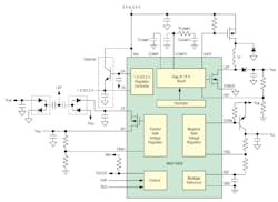
An example of a highly integrated power supply for automotive TFT-LCD applications is the Maxim MAX16928 (Fig. 8-22). The IC integrates a boost converter, 1.8V/3.3V regulator controller, positive-gate voltage regulator, and negative-gate voltage regulator.
8-22. Maxim’s MAX16928 powers TFT LCDs with integrated boost converter, 1.8V/3.3V regulator controller, positive-gate voltage regulator, and negative-gate voltage regulator.
It achieves enhanced EMI performance through spread-spectrum modulation. Digital input control allows the device to be placed in a low-current shutdown mode and provides flexible sequencing of the gate voltage regulators.
Internal thermal shutdown circuitry protects the IC. It will shut down if its die temperature reaches +165°C (typ) and will resume normal operation once its die temperature falls 15°C.
It is factory-trimmed to provide a variety of power options to meet the most common automotive TFT-LCD display power requirements.
Its boost converter employs a current-mode, fixed-frequency PWM architecture to maximize loop bandwidth and provide fast transient response to pulsed loads typical of TFT-LCD panel source drivers. The 2.2MHz switching frequency allows use of low-profile inductors and ceramic capacitors that minimize thickness of LCD panels. An integrated low on-resistance MOSFET and the IC’s built-in digital soft-start functions reduce the required number of external components while controlling inrush currents. Using an external resistive voltage-divider you can set output voltage from VINA to 18V. The regulator controls the output voltage by modulating the duty cycle (D) of the internal power MOSFET in each switching cycle.
Features
- Up to 6W Boost Output Providing Up to 18V
- 1.8V or 3.3V Regulator Provides 500mA with External NPN Transistor
- One Positive-Gate Voltage Regulator Capable of Delivering 20mA at 28V
- One Negative-Gate Voltage Regulator
- 2.2MHz Switching Operation
- Flexible Stand-Alone Sequencing
- True Shutdown Boost Converter
- Internal Soft-Start
- Overtemperature Shutdown
- -40°C to +105°C Operation
- AEC-Q100 Qualified
Multi-Channel Power Management ICs
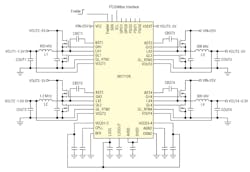
The XR77128 from Exar (now MaxLinear) is a quad-channel digital Pulse Width Modulated (PWM) step-down (buck) controller (Fig. 8-23). A wide 4.75V to 5.5V and 5.5V to 25V input voltage range allows for single supply operation from standard power rails.
8-23. Exar’s XR77128 is a four-channel digital PWM step down (buck) controller.
With integrated FET gate drivers, two LDOs for standby power, and a 105kHz to 1.23MHz independent channel-to-channel programmable constant operating frequency, the XR77128 reduces overall component count, solution footprint, and optimizes conversion efficiencies. A selectable digital Pulse Frequency Mode (PFM) capable of better than 80% efficiency at light current load and low operating current allow for portable and Energy Star compliant applications. Each XR77128 channel’s output voltage is individually programmable down to 0.6V with a resolution of 2.5mV, and is configurable for precise soft start and soft stop sequencing, including delay and ramp control.
The XR77128 operations are fully controlled via a SMBus-compliant I2C interface, allowing for advanced local and/or remote reconfiguration and full performance monitoring and reporting as well as fault handling.
Built-in independent output Over-Voltage, Over-Temperature, Over-Current, and Under-Voltage Lockout protections insure safe operation under abnormal operating conditions.
MIC7400
The MIC7400 from Micrel is a multi-channel power supply with internal EEPROM (Fig. 8-24). It offers software-configurable soft-start, sequencing and digital voltage control (DVC) that minimizes PC board area. MIC7400 buck regulators are adaptive on-time synchronous step-down dc-dc regulators that operate from a 2.4V to 5.5V input range.
8-24. Micrel’s MIC7400 is a multi-channel power supply with internal EEPROM.
IC Features
- Five independent synchronous buck converters up to 3A
- One independent non-synchronous boost converter to 200mA and 70µA quiescent current
- 200µA quiescent current with all regulators on
- 93% peak buck efficiency, 85% typical efficiency at 1 mA
- 2.0MHz boost switching frequency
- 1.3 MHz buck operation in continuous mode
- Thermal shutdown and current limit protection
Programmable features
- Buck output voltage: 0.8V to 3.3V in 50 mV steps
- Boost output voltage: 7.0 to 14V in200 mV steps
- Power on reset: 2.25V to 4.25V in 50 mV steps
- Power on reset delay: 5ms to 160ms in 5ms steps
- Power-up sequencing: 6 time slots
- Power-up sequencing delay: 0ms to 7ms in 1ms steps
- Soft-start: 4µs to 1024µs per step
- Buck current limit threshold: 1.1A to 6.1A in 0.5A steps
- Boost current limit threshold: 1.76A to 2.6A in 0.12A steps
- Boost pull-down: 37mA to 148mA in 37mA steps
- Buck pull-down: 90Ω
- Buck standby output voltage programmable
- Boost standby output voltage programmable
- Global power good masking
Read more articles from the Power Management Series in the Power Management section of our Series Library.

