This file type includes high resolution graphics and schematics.
Capacitor-based charge pumps (or Q-pumps) generally aren’t useful for sourcing large amounts of current, but they work well in niche micropower applications where space is at a premium. They work best in applications where the output voltages are integer multiples of the input voltage. The integer multiples, then, are operating points that result in peak efficiency.
However, Q-pumps can also work well when they are powered from a variable input such as a battery, particularly when quiescent battery drain is more important than heavy-load efficiency. This might be the case when powering a microcontroller that spends most of its time in sleep mode.
Low-voltage microcontrollers such as those in the PIC24 or MSP430 families are generally powered from a regulated supply voltage such as 2.5 V. If clocked slowly, they might draw as little as 25 μA or 50 μA. In standby mode with only the real-time clock running, the current can be vanishingly small, often less than a microamp. This is a good application for the regulated two-stage Q-pump described here, which boosts a single alkaline or nickel-metal-hydride (NiMH) cell to 2.5 V.
The “wings” of a Q-pump, called “flying capacitors,” connect first to the input and then to the output. If the capacitor is stacked on the input voltage, it forms a voltage doubler. In the case of a regulated charge pump with a fixed output voltage, the voltage across the flying capacitor may differ significantly from the voltage across the output-filter capacitor.
When you connect two capacitors that are initially charged to different voltages, you get a spark or power dissipation in the switches as the capacitors equalize in voltage. This is why a simple voltage doubler typically exhibits better efficiency than a regulated Q-pump.
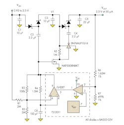
This regulated Q-pump has an on-demand oscillator, a feedback regulation loop made from an op amp and reference, and a two-stage pump circuit, plus two flying capacitors, C2 and C4 (Fig. 1). The first pump stage is driven directly by the Touchstone Semiconductor TS12011 comparator, which forms the oscillator, while the second stage is driven by an inverter powered from the output voltage of the first stage. The full-load efficiency varies from 70% to 40% over a 1- to 2.5-V input range, which is comparable to a linear regulator.
The TS12011 analog building block requires very low supply currents (3.2 μA typical ) and operates well down at the sub-1-V levels needed for single-cell operation. The comparator output stage has good drive-current capability down below 0.8 V VDD, an uncommon feature that allows us to drive the first stage directly from the oscillator.
The SN74AUP family of logic gates similarly uses super-low power. The MOSFETs were also carefully chosen for low-voltage operation, with low gate-threshold voltage specifications and low gate-charge characteristics for low switching losses. Using these high-performance components, the no-load quiescent current is a mere 8 μA.
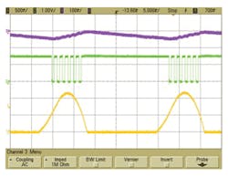
The RC oscillator is stopped when the output is in regulation via its /LHDET latch input (Fig. 2). When the output is above the regulation threshold set by the reference and feedback divider, the op-amp output drives the latch input low, latching the comparator output in the high state and stopping the oscillator.
A large hysteresis band was chosen for the oscillator, resulting in a large signal swing on the timing capacitor C6. This achieves the most efficient size-versus-current operating point for the oscillator. The maximum frequency is nominally set at 1 kHz with the component values shown, but can be adjusted up to about 3 kHz, where it becomes limited by the propagation delay through the comparator.
The amount of charge transferred with each cycle and the switching frequency determine the output current. Accurate calculations for the output impedance or output current from a regulated two-stage pump are complex and need a large spreadsheet, but you can make some oversimplifications to get into the right range. Assuming the capacitor is completely charged and discharged with each cycle (which obviously isn’t true), then:
Q = C × V
I = Q × f
so:
I = C × V × F
where C is the flying capacitor value, V is the applied voltage during the charging phase, F is the oscillator frequency, and I is the output current you’d get if you could remove all the stored charge during the discharge phase (roughly equivalent to a short-circuit load current).
This file type includes high resolution graphics and schematics.
The modified Dickson Multiplier two-stage pump topology used here is a quadrupler, and both stages must be designed to transfer the needed amount of charge at the worst-case low-battery voltage. The first stage is the most important, because the voltage applied to the capacitor is low. Any drop across the first rectifier subtracts from the applied voltage with a resulting loss in headroom, a problem when trying to multiply up to 2.5-V output levels.
The rectifier choice is further complicated in this low-quiescent application by leakage currents, which effectively load down the pump and increase idling current. The BAS52-02V Schottky diode has a good combination of low reverse leakage, low forward drop, small packaging, and wide availability.
Reverse leakage current at high temperature is the weakness of Schottky diodes, but lab measurements show that the typical BAS52 is very good on this parameter, at less than 1 μA at 50°C. For even lower reverse leakage, there is the BAS40-02V, but the tradeoff is about 75-mV higher forward-voltage drop.
The capacitor values and switching frequency are chosen to be somewhat excessive for charge transfer, so they don’t get in the way of the voltage-drop/headroom issues. As a result, the frequency is low and the capacitors are relatively large, which also keeps switching losses in check. More importantly, a long on-time allows the voltage across the diode to reach a minimum, with the tail end of the forward voltage/current curve being a little less than 0.2 V for the BAS52.
From the simplified charge-transfer equations above, an overly optimistic estimate for first-stage current is:
(VDD – VFWD – VSAT1) × C3 × F = (0.95 V – 0.2 V – 0.05 V) × 2.2 μF × 1 kHz = 1.5 mA
which is more than sufficient to meet a 50-μA load-current requirement. The best-possible peak-output voltage that you can achieve for the intermediate V1 tap is:
2VDD – 2VFWD – VSAT1(high) – VSAT1(low)
Similarly, the second-stage peak voltage for VOUT is:
2V1 – 2VFWD –VSAT2(high) – VSAT2(low)
Thus, the best-possible peak-load voltage at the minimum input voltage is:
VOUT = 4VDD – 4VFWD – 4VSAT = (4 × 0.95 V) – (4 × 0.2 V) – (2 × 0.05 V) – (2 × 0.1 V) = 2.7 V
where VSAT1 and VSAT2 are the voltage drops across the comparator and the AUP inverter output stages in the ON state, respectively. Again, this analysis is oversimplified but points out the limits of operation.
This math shows that there is not a lot of room for temperature variation and component tolerances when trying to quadruple the lower end of the voltage range of a single cell. We can improve this, and get to sub-0.9 V operation, by several means: adding another pump stage; changing the output voltage to 2.2 V (but the microcontroller may not be able operate this low); or adding a synchronous rectifier across the first diode.
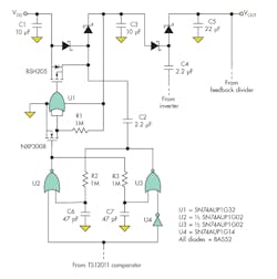
The third option is chosen here, due to its good efficiency at the operating “sweet spots” (Fig. 3). A low-threshold P-channel MOSFET with low gate charge shunts the first pump diode, reducing the forward drop from 0.2 V to approximately 0.01 V. This adds a few hundred extra millivolts right at the front end, where it’s needed most.
A NOR-based logic circuit provides non-overlapping gate-drive signals to the synchronous switch. The goal is to be certain that the MOSFET gate is never driven high when the flying capacitor is high. The amount of dead time is set by the 1 MΩ × 47 pF RC time constants. Here, the dead time is very long since the 1-kHz oscillator is so slow.
Charge pumps offer an alternative to inductor-based boost regulators and can fit nicely with the dual nature of many microcontroller loads, with their low-current RTC mode versus heavier but infrequent run mode. The challenge of designing them for low input voltages can be met by using the right low-voltage components, choosing sensible switching frequencies, and taking full advantage of the V-I characteristics of the rectifiers.


