Thermal management in semiconductor applications often makes it tough to optimize performance. Synthetic chemical-vapor-deposition (CVD) diamond helps overcome those limitations by significantly lowering gate junction temperatures, thus enhancing power densities and efficiencies as well as extending lifetimes. As technology and economic drivers push systems to higher frequencies, higher voltages, and higher ambient operating temperatures, synthetic diamond heat spreaders and gallium-nitride (GaN)-on-diamond wafers will see increased use in thermal-management schemes for high-power semiconductor devices.
Synthetic CVD diamond’s room-temperature thermal conductivity runs as high as 2000 W/mK, five times that of copper and 10 times that of aluminium nitride. Further, because diamond transports heat equally well in all three dimensions, it can act as an excellent heat spreader. Both metallized diamond heat spreaders and GaN-on-diamond wafers have been shown to drastically lower thermal resistance and, in turn, the gate junction temperature of semiconductor devices, leading to higher power densities.
High-Power RF
High-power radio-frequency (RF) power amplifiers are used in military and commercial applications such as radar systems, electronic warfare, and cellular base stations. The latest high-power RF PAs consist of GaN epitaxial material, which performs exceptionally well at higher frequencies, boosts efficiency, and handles higher power densities.
However, these GaN RF devices have very small hotspots that can generate heat fluxes 10 times that of the sun’s surface. As a result, thermal-management challenges often severely limit their intrinsic performance advantages. GaN-on-diamond wafers eliminate this thermal limitation by bringing the diamond within less than one micron from the heat-generating gate junction.
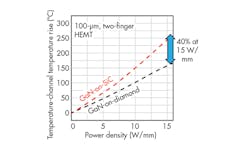
In one example, TriQuint fabricated identical HEMT’s (high electronic mobility transistors) on GaN-on-diamond substrates and GaN-on-SiC substrates. The University of Bristol used micro-Raman methodology to measure thermal resistances of the two transistor types, and found that the thermal resistance of the GaN-on-diamond HEMTs was at least 40% lower than that of the GaN-on-SiC HEMTs1(Fig. 1).
GaN-on-diamond technology offers two key benefits. First, it enables devices that are more than three times smaller than with other approaches, making them less expensive and providing much more power in a smaller form factor.2 Second, devices are able to run in ambient temperatures as much as 50% hotter, thereby lowering the cost of cooling subsystems and ultimately saving on-going energy expense.
This file type includes high resolution graphics and schematics when applicable.
High-Voltage Power Devices
High-voltage power devices, such as insulated-gate bipolar transistors (IGBTs), have the advantage of higher efficiency and higher switching frequencies, but generate significant heat that demands extreme thermal-management solutions. For IGBTs, an effective thermal-management solution once again is to bring diamond as close to the heat-generating source in the form of metallized heat spreaders.
High-voltage IGBT applications typically involve switching or converting power for electrical vehicles, train and aerospace power generators, and alternative-energy distribution. In one test case using a 1200-V IGBT, a metallized diamond heat spreader replaced a ceramic substrate. It more than halved the junction-to-case thermal resistance, which in turn more than doubled the IGBT’s power rating.
Growing Single-Crystal Diamond Substrates for Power Devices
By Don Tuite
Power semiconductors that need to carry high voltages and dissipate high power losses require synthetic single-crystal diamond material. A few companies do that by growing electronics-grade diamond at a few percent of atmospheric pressure in an ionized bath of hydrocarbons and hydrogen. For most producers, however, the process starts with a tiny seed of diamond, although some experimentation is now occurring with iridium. The seed material isn’t incorporated into the final substrate material; the seed substrate can actually be reused again and again.
In the process, the seed substrate is heated to a temperature between 700 and 1000ºC in a mixture of a carbon-based gases that includes methane, ethane, or ethylene and hydrogen—a less toxic mix than the metal-organics used in making some III-V semiconductor materials.
When a powerful microwave sources ionizes the gas mixture, diamond grows on top of the seed. The higher the microwave power, the faster the growth. The approach has achieved rates up 200 microns per hour. Defect rates are currently on the order of 102 per cubic centimeter.
Diamonds are particularly helpful in the fact they have only one possible crystal structure—a simple cube of eight atoms. As a result, crystal defects tend not to tend to propagate.
To obtain a large enough substrate on which to fabricate power-electronics devices, suppliers create larger-area substrates through a "tiling" process. This involves a mosaic of cut and polished single-crystal diamonds assembled into a tightly packed, flat array. Tiling is made possible via growth reactors that can produce 100-mm wafers.
“Scaling to this area for single wafers can be accomplished relatively painlessly,” says eVince Technology (evincetechnology.com). “For practical applications, achieving high-yield production does not require a 100% defect-free substrate, so long as the wafer has a regular grid-iron pattern of high-quality areas of low-defect single-crystal diamond.”
Again, in the reactor, the mosaic is heated to between 700 and 1000ºC in a mixture of either methane or ethylene and hydrogen at around 1.0 atmosphere. The microwave source ionizes the gas into a plasma that liberates carbon from whichever gas is used.
The carbon atoms bind with the seed substrate to form new diamond. As the diamond film grows, it generally matches up the crystal pattern at the tile boundaries to form a homogenous single-crystal diamond substrate. Some boundary defects are inevitable, but the thicker the growth layer, the lower the percentage of tiling defects. Layers as thick as 10 mm and more have been successfully grown, according to eVince.
The final step is to save the seed layer for further use. Before starting the new growth, a graphite “damage layer” was applied on top of the seed layer. After deposition, the newly grown laminations of diamond film can then be separated from the tiled seed substrates, which can then be reused.
eVince says that “by cycling the implantation and growth stages, multiple free-standing substrates can be produced in the same growth run. These substrates can then be either used for device production, or the ones with the fewest edge defects can be used as starter tiles to create even larger substrates.”
Laser Diode Arrays
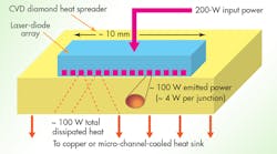
High-power laser-diode arrays are found in material processing (e.g., welding and surface treatments), medical applications (e.g., tattoo removal and laser surgery), and applications for pumping high-power solid-state lasers. These arrays require significant thermal management to optimize performance. Adding a diamond heat spreader between the diode array and the submount effectively transports the heat away from small emitter hotspots.
However, the coefficient of thermal expansion (CTE) mismatch between the diamond heat spreader and the laser-diode gallium arsenide (GaAs) can cause reliability issues, as well as the condition known as a “smile”—a slight bend of the horizontal line connecting the emitters. On-going research and development efforts are on ways to effectively solve this CTE-mismatch issue.
Figure 2 shows a 100-W laser-diode array with multiple emitters closely spaced on a single chip. The light output from these emitters is either used directly or collimated with a lens array into a single-beam laser. High power output, wavelength stability, and reliability of these arrays are of utmost importance.
Using metallized heat spreaders to cool laser-diode arrays can significantly increase beam intensity and beam quality, since it allows for closer spacing of the individual emitters in the arrays. In addition, or alternatively, diamond heat spreaders can extend the lifetime of the diode arrays.
Semiconductor Assembly and Test
Certain steps in the test and assembly of packaged semiconductor devices requires that temperature either be kept low enough to prevent device damage, or kept constant across the entire package for optimum assembly quality. Because metallized diamond heat spreaders can transport heat both laterally and vertically at very fast rates, they’re able to rapidly pull heat away from, and spread it evenly across, hot devices.
One example involves cooling of devices during functional test. The device under test needs to operate under a test pattern without a heat sink attached, which may cause it to quickly overheat. Using CVD diamond effectively addresses this cooling issue without resorting to active water impingement cooling.
In another case, using diamond to rapidly spread heat across a substrate while a flip-chip die is being bonded to it makes it possible to apply the same amount of heat to every solder joint at the same time. This ensures high-quality across an array of 1000 solder joints.
Bruce Bollinger leads worldwide business development for synthetic diamond applications at Element Six Technologies. He has over 20 years of experience in manufacturing, business development and marketing, as well as seven years of operations management experience in Asia. Bruce obtained a BSEE from Washington University in St. Louis, and completed his MBA at the Harvard Business School.
Thomas Obeloer, business development manager at Element Six Technologies, holds a Master’s degree in mechanical engineering. He has more than 20 years’ experience with advanced thermal management, mainly in the field of advanced materials such as CVD Diamond.
References:
1. D.C. Dumka, T.M. Chou, J.L. Jimenez, D.M. Fanning, D. Francis, F. Faili, F. Ejeckam, M. Bernardoni, J.W. Pomeroy, and M. Kuball, TriQuint, “Electrical and Thermal Performance of AlGaN/GaN HEMTs on Diamond Substrate for RF Applications,” in 35th IEEET Compound Semiconductor IC Symposium (CSICS) Oct. 13-16, 2013, Monterey, CA, Section F.4.
2. M. Tyhach, D. Altman, and S. Bernstein, Raytheon, “Analysis and Characterization of Thermal Transport in GaN HEMTs on SiC and Diamond Substrates”, in GOMACTech 2014, March 31-April 3, 2014, Charleston, SC.
3. J.Anaya, J.W. Pomeroy, and M. Kuball, ELEMENT-6, “GaN-on-Diamond High-Electron-Mobility Transistor—Impact of Contact and Transition Layers,” Center for Device Thermography and Reliability (CDTR), H. H. Wills Physics Laboratory, University of Bristol, BS8 1TL, Bristol, U.K.


