IR-Triggered MEMS Switch Requires Zero Power When Dormant
Even the minute amount of current needed in slow, infrequently activated Internet of Things (IoT) and other sensing applications can aggregate to an unacceptable energy drain and associated battery depletion, or result in energy-harvesting challenges. To address this issue, a team at Northeastern University has developed a MEMS-based switch that consumes zero power when it’s in dormant standby mode, but will “wake up” when triggered and subsequently turn on the rest of the circuitry.
The event-driven switch is activated by impinging infrared (IR) light, and transforms the tiny amount of photonic energy within defined spectral bands to activate a MEMS mechanism. This IR energy could be from a source such as a flame or explosion; when the activating IR energy is removed, the switch turns itself off.
The physics of transforming the IR absorption is based on plasmons, which are the waves of electrons that move along the surface of a metal after it’s been struck by photons. Plasmonic principles allow for the efficient absorption of light, as well as enable its selective spectral absorption. Therefore, different IR wavelengths could be used to activate different switches, even in the same chip.
Plasmonic Switches
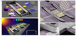
Dubbed plasmonically enhanced micromechanical photoswitches (PMPs), the devices are based on nanoscale gold patches. The plasmonic absorber is fabricated as a three-material stack, with a 100-nm dielectric layer sandwiched within an array of 50-nm gold nano-patches on the top, and a 100-nm platinum plate on the bottom (see figure). The switches are packaged in a vacuum to eliminate interference from other molecules and provide thermal isolation.
The switches take energy from the IR electromagnetic radiation at specific, targeted wavelengths, and use it to mechanically close the contacts of the switches, thus creating a low-resistance electrical path without a need for any other power source. The activation mechanism is electromagnetic-to-thermal energy conversion.
The optical energy of infrared light that hits the device is absorbed by the integrated, ultra-thin plasmonic infrared layers and converted into heat. This raises the temperature of a dual-material structure (analogous to a conventional bimetallic strip), which then bends and moves one piece of metal into contact with the other.
The Northeastern University researchers call these infrared sensors “digitizing” devices, because they have well-defined, sharp activation thresholds and are either in an on or off state. Unlike other IR sensors, they don’t indicate the amount of IR radiation received.
They reported that the devices had a large and sharp off-to-on state-transition slope of above nine decades/nW. On/off conductance ratio was greater than 1012 when exposed to infrared radiation in a specific narrow spectral band (∼900-nm bandwidth in the mid-infrared) and with the intensity above a modest power threshold of only ∼500 nW.
The published paper, “Zero-power infrared digitizers based on plasmonically enhanced micromechanical photoswitches,” is in the October 2017 issue of Nature Nanotechnology and provides full technical details.


