Some applications require the monitoring of power applied to a system. Microchip Technology addressed this need with the MCP39F511A, a highly integrated, single-phase power-monitoring IC intended for real-time measurement of ac and dc inputs. It detects the input voltage and automatically sets operation in the appropriate mode, either dc or ac.
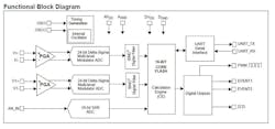
Separate ac and dc calibration registers help ensure high-accuracy measurements in both modes. An integrated 7-ppm/°C voltage reference and 94.5-dB signal-to-noise and distortion ratio (SINAD) performance are employed in each mode. The IC provides 0.1% accuracy over a 4000:1 dynamic range. Housed in a 28-lead 5×5 QFN package, it has an operating temperature range of −40 to +125°C. Figure 1 shows a simplified block diagram of the MCP39F511A.
1. Shown is a simplified block diagram of the MCP39F511A.
The MCP39F511A includes an asynchronous full-duplex UART with eight Start and Stop bits and a default baud rate of 9.6 kb/s. The Simple Sensor Interface (SSI) protocol is used for point-to-point communication from a single-host microcontroller (MCU) to a single-slave MCP39F511A. The UART communication provides the monitoring data to the MCU, which can be displayed on a monitor or printed out.
All communication to the MCP39F511A occurs in frames that consist of a header byte, the number of bytes in the frame, command packet (or command packets), and a checksum. The maximum number of bytes for either a receive or transmit frame is 35 (Fig. 2). This approach allows for single, secure transmission from the host processor to the MCP39F511A with either a single command or multiple commands.
2. Communications to the MCP39F511A occur in frames.
After the reception of a communication frame, the MCP39F511A has three possible responses, which will be returned with or without data depending on the frame received. These responses are:
- Acknowledge (ACK, 0x06): Frame received with success, commands understood, and commands executed with success.
- Negative Acknowledge (NAK, 0x15): Frame received with success, however commands not executed with success, commands not understood, or some other error in the command bytes.
- Checksum Fail (CSFAIL, 0x51): Frame received with success, however the checksum of the frame did not match the bytes in the frame.
A list of all accepted command bytes for the MCP39F511A includes:
- Register Read, N Bytes (0x4E)
- Register Write, N Bytes (0x4D)
- Set Address Pointer (0x41)
- Save Registers To Flash (0x53)
- Page Read EEPROM (0x42)
- Page Write EEPROM (0x50)
- Bulk Erase EEPROM (0x4F)
- Auto-Calibrate Gain (0x5A)
- Auto-Calibrate Reactive Power Gain (0x7A)
- Auto-Calibrate Frequency (0x76)
- Save Energy Counters To EEPROM (0x45)
Coherent Sampling Algorithm
The MCP39F511Auses a coherent sampling algorithm to phase lock the sampling rate to the line frequency with an integer number of samples per line cycle (56) and reports all power output quantities at a 2N number of line cycles. Defined as a computation cycle, it’s dependent on the line frequency. Thus, any change in the line frequency will also change the update rate of the power outputs.
Assuming that the input frequency is 60 Hz, the sampling speed is 56 × 60 = 3360 samples/s. For the default accumulation interval parameter of 2, the computational cycle is 56 × 4 divided by the sampling speed (the result is 66.66 ms). In dc mode, the sampling speed is fixed at approximately 1953 samples/s. For the default value of the accumulation interval parameter (2), the computational cycle is 56 × 4 divided by the sampling speed (the result is approximately 114.7 ms).
The coherent sampling algorithm is also used to calculate the Line Frequency Output register, which is updated every computation cycle. The correction factor for line frequency measurement is the Gain Line Frequency register, which is used during the line frequency calibration. The resolution of the Line Frequency Output register is fixed, and the resolution is 1 mHz.
At Power-on Reset, the calculation engine must initialize the analog front end (AFE) and initialize all of the peripherals prior to being able to start the first computation cycle. In addition, the device must detect whether or not an ac signal is present; if so, it must determine the correct coherent sampling clock values. This process is given sufficient time for correct initialization; the startup time is 417 ms for a 60-Hz line.
Its high-pass filters are turned off to let pass both dc and ac signals. If the number of zero crossings detected during this time on the voltage channel is less than 10 (to filter out false detections), the device will automatically switch to dc mode.
An internal counter based on the sampling rate of the AFE determines if an ac signal isn’t present and if the device should switch to dc mode. If an ac signal isn’t present for this time period (same as above, based on the number of zero crossings detected on the voltage channel), the device will switch to dc mode, turning off the high-pass filters and setting the frequency output to zero.
The accumulation interval is defined as a 2N number of line cycles, where N is the value in the Accumulation Interval Parameter register. N can be as low as 0 (for the fastest update rate), but no bigger than 8.
Several registers are used to store data, including:
- System Status register
- Address Pointer register
- System Version register
- System Configuration register
- Range Register
RMS Measurements
The MCP39F511A provides true RMS measurements. It has two simultaneous sampling 24-bit A/D converters for the current and voltage measurements. The root mean square calculations are performed on 2N current and voltage samples, where N is defined by the register Accumulation Interval Parameter
For active and reactive power, import and export registers for active energy, and four-quadrant reactive power measurement the MCP39F511A offers signed power numbers. Import power or energy is considered positive (power or energy being consumed by the load), and export power or energy is considered negative (power or energy being delivered by the load).
Energy accumulation for all four energy registers (Import/Export, Active/Reactive) occurs at the end of each computation cycle, if the energy accumulation has been turned on. A no-load threshold test is done to make sure the measured energy is not below the no-load threshold, if it is above, the accumulation occurs with a default energy resolution of 1 mWh for all of the energy registers.
The no-load threshold is set by modifying the value in the No-Load Threshold register. The unit for this register is power with a default resolution of 0.01W. The default value is 100 or 1.00W. Any power that is below 1W will not be accumulated into any of the energy registers.
A 32-bit register stores the final apparent power indication. It is the product of RMS current and RMS voltage. For scaling of the apparent power indication, the calculation engine uses the register Apparent Power Divisor Digits.
For the active power calculation, the instantaneous current and instantaneous voltages are multiplied together to create instantaneous power.
This instantaneous power is then converted to active power by averaging or calculating the DC component. Although this register is unsigned, the direction of the active power (import or export) can be determined by the Active Power Sign bit located in the System Status Register.
Power factor is calculated by the ratio of active power divided by apparent power. The power factor reading is stored in a signed 16-bit register (Power Factor). This register is a signed, 2's complement register with the MSB representing the polarity of the power factor. A positive power factor means Active power is being imported, a negative power factor represents export active power. The sign of the reactive power component is used to tell if the current is lagging the voltage, with a positive sign meaning an inductive load and a negative sign meaning capacitive. Each LSB is then equivalent to a weight of 2-15.
Reactive power is calculated using a 90 degree phase shift in the voltage channel. The same accumulation principles apply as with active power where ACCU acts as the accumulator. Any light load or residual power can be removed by using the Offset Reactive Power register. Gain is corrected by the Gain Reactive Power register. The final output is an unsigned 32-bit value located in the Reactive Power register. This register is unsigned, the direction of the power can be determined by the Reactive Power Sign bit in the system Status register.
Pulse Width Modulation
The PWM output pin gives up to a 10-bit resolution of a PWM signal. The PWM output is controlled by an internal timer inside the MCP39F511A, FTIMER, with a base
frequency of 16 MHz. The base period is defined as PTIMER and is 1/[16 MHz]. This 16-MHz time base is fixed due to the 4-MHz internal oscillator or 4-MHz external quartz crystal.
Two registers control the PWM output, PWM period, and PWM duty cycle. The 8-bit PWM period is controlled by a 16-bit register that contains the period bits as well as the prescaler bits. The PWM period bits are the most significant eight bits in the register; the prescaler value is represented by the least two significant bits. These two values together create the PWM period. The 10-bit PWM duty cycle is controlled by a 16-bit register where the eight most significant bits are the 8 MSBs and the 2 LSBs, corresponding to the 2 LSBs of the 10-bit value.
Calibration
Calibration compensates for the ADC gain error, component tolerances, and overall noise in the system. The device provides an on-chip calibration algorithm that enables simple system calibration to be performed quickly. The excellent analog performance of the ADCs on the MCP39F511Aallows for a single-point calibration and a single calibration command to achieve accurate measurements in ac mode. In dc mode, offset calibration is usually required.
Calibration can be done by either using the predefined auto-calibration commands, or by writing directly to the calibration registers. If additional calibration points are required (ac offset, phase compensation, dc offset), the corresponding calibration registers are available.
Power Monitor Demonstration Board
The MCP39F511A Power Monitor Demonstration Board is a fully functional, single-phase power and energy monitor (Fig. 3). The system calculates active power, reactive power, RMS current, RMS voltage, active energy (both import and export), reactive energy, and other typical power quantities.
3. The MCP39F511A single-phase power and energy monitor demo board has an internal 3.3-V switching power supply and isolated UART inputs from the MCU.
This Power Monitor Demonstration Board uses the Power Monitor Utility software for evaluation through a USB connection to the board. The Utility software is used to calibrate and monitor the system, and can be used to create custom calibration setups. For most accuracy requirements, only a single-point calibration is needed. The software offers an automated step-by-step calibration process that can be used to quickly calibrate power meters.
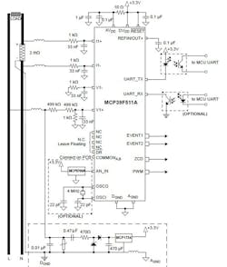
The Demonstration Board operates from 90 to 230 V rms. The high-voltage line and neutral connections are located at the bottom of the board. The shunt sits on the neutral or the low side of a two-wire system.
The board comes populated with a surface-mount 2-mΩ shunt. When using a lower value external shunt, twist together the wires going from the external shunt to the CP1 and CP2 connections. The high-voltage side of the two-wire system goes into a resistor divider on the voltage-channel input. Anti-aliasing low-pass filters are inserted on the input pins. The voltage channel uses two 499-kΩ resistors to achieve a divider ratio of 1000:1. For a line voltage of 220 V rms, the channel 1 input signal size is 220 mV rms.


