GaN Power Transistors: Master Strokes on a Power-Supply Canvas
Download this article in PDF format.
It’s not news that the efficiency of switching power supplies is now above 90% in many applications. At those levels, it becomes progressively harder to eke out small improvements.
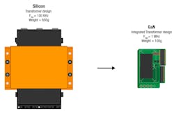
The introduction of power devices made from wide-bandgap (WBG) semiconductors such as gallium nitride (GaN) and silicon carbide (SiC), instead of silicon, has given designers some important new tools (Fig. 1).
1. Changing from silicon to GaN in a power supply can slash the size of magnetic components such as transformers. (Source: TI: “Gallium Nitride (GaN): Pushing performance beyond silicon”)
Sponsored Resources:
- Power Supply Design Seminar Training Series
- Survey of Resonant Converter Topologies
- Comparison of GaN and Silicon FET-Based Active Clamp Flyback Converters
In a power supply, changing from silicon MOSFETs to transistors based on gallium nitride (GaN) yields efficiency improvements. A GaN device (Fig. 2) has lower on-resistance RDS(ON) than a silicon device. It also has a higher breakdown voltage, can operate at higher temperatures, and has far superior reverse-recovery characteristics. The GaN device also incurs much lower switching losses, so it can operate at higher switching frequencies. As shown in Fig. 1, this can lead to a dramatic reduction in the size of the design.
2. Wide bandgap semiconductors such as GaN and SiC offer superior performance over silicon in power applications.
Higher switching frequencies reduce power converter size, weight, and cost because they allow the use of smaller capacitors, inductors, and transformers. Switching to GaN power devices can cut the size of a power supply by up to 50%.
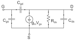
Let’s examine in more detail the advantages of switching to GaN, beginning by reviewing the simplified high-frequency model of a power MOSFET in Figure 3. This model applies to both silicon and GaN technologies.
3. A simplified high-frequency equivalent circuit of a MOSFET. (Source: Author)
It includes parasitic junction capacitances CGD, CGS, and CDS. In the datasheet, these are stated as the input capacitance (CISS), the output capacitance (COSS), and the reverse transfer capacitance (CRSS), where:
CRSS = CGD
CISS = CGS + CGD
COSS = CDS + CGD
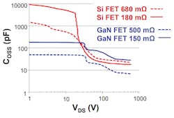
The parasitic junction capacitances are formed from a series combination of a bias-independent oxide capacitance and a bias-dependent depletion capacitance. COSS decreases for lower values of RDS(ON). For a given device, COSS is also nonlinear and decreases significantly above a VDS threshold.
The shape of the curve is significantly different for Si and GaN devices. As shown in Figure 4, for a GaN FET, COSS is proportional to RDS(ON) and varies very little for VDS < 30 V.
4. Variation of COSS with VDS and RDS(ON) for GaN and Si FETs. (Source: TI: “Comparison of GaN- and Silicon FET-Based Active Clamp Flyback Converters” PDF, p. 6)
For a silicon FET, on the other hand, COSS steadily increases as VDS decreases below 30 V, but the increase isn’t proportional to RDS(ON). For the device in Figure 4 with RDS(ON) = 680 mΩ, COSS at VDS = 30 V is about 100X larger than its value at VDS = 400 V. For another device with RDS(ON) = 180 mΩ, COSS is almost 300X larger over the same VDS range.
A silicon MOSFET also has a body diode—it’s an intrinsic PN junction formed during the manufacturing process. One consequence of the body diode is an undesired reverse-recovery charge when the diode turns off. GaN FETs don’t have an intrinsic body diode, so there’s zero reverse-recovery charge.
Application Example: The Active Flyback Converter
As we can see, the characteristics of Si and GaN devices are significantly different, but how does changing from silicon to GaN improve performance in a power supply? Let’s use the active-clamp flyback (ACF) converter as an example. The ACF is a popular choice for small power adapters because it combines high power density with high efficiency.
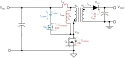
Figure 5 shows the ACF circuit. The active clamp consists of a high-side secondary switch (QH) in series with a clamp capacitor (CCLAMP). This circuit uses silicon devices, hence the body diodes.
5. The active-clamp flyback converter, showing the MOSFET body diodes and some of the equivalent circuits.
Also shown in Fig. 5 are some essential equivalent circuit elements: the output capacitances (COSS) for QH and QL; and the secondary rectifier capacitance (CSEC). The transformer can be modeled as a transformer leakage inductance (LLK) in series with a primary-side magnetizing inductance (LPM).
The purpose of the active clamp is to recycle the energy stored in the transformer leakage by storing it in CCLAMP. The circuit then delivers the energy to the output later in the switching cycle to minimize the voltage spike at the transformer primary side, thus reducing the voltage stress on the main switch QL.
Controlling the timing of the active clamp switch can also eliminate switching loss by turning on QL at the zero-volt switching point (ZVS operation). ZVS operation allows the ACF switching frequency to be higher, reducing the size of the power supply.
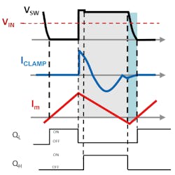
Figure 6 shows the switching events in the ACF sequence, beginning with primary power switch QL and clamp switch QH both off. Note that both ICLAMP and IM are bidirectional as shown in Fig. 5 above: the direction is denoted in the discussion by, for example, IM(+) and IM(-).
6. The principal currents and voltages of the ACF during a ZVS switching cycle. (Source: TI: “Comparison of GaN- and Silicon FET-Based Active Clamp Flyback Converters” PDF, p. 2)
A summary of the active-clamp ZVS operation follows. Consult this paper for an in-depth discussion.
- QL turns on: IM(+) is linearly increasing, storing energy in the primary-side magnetizing inductance LPM.
- QL turns off: IM(+) charges the junction capacitance of QL (COSS(QL)) and discharges both the junction capacitance of QH, (COSS(QH)) and the junction capacitance of the secondary rectifier (CSEC). Therefore, the current on QL (IQL) decreases, the clamp current (ICLAMP) increases, and the secondary rectifier current (IS) increases with VSW rising from 0 V to a high level. IM(+) flows through the body diode of QH to charge CCLAMP.
- QH turns on: QH is conducting, NVOUT starts to demagnetize LPM, so IM(+) starts to decay, and LPM releases its energy to the output. At the same time, CCLAMP absorbs the LLK energy by resonating with LLK; therefore, ICLAMP is in the positive direction.
- QH turns off: The negative magnetizing current, IM(-), starts to discharge COSS(QL), charge COSS(QH), and charge the CSEC, so VSW decays to 0 V.
- The sequence then repeats: QL turns on as VSW reaches 0 V, giving ZVS operation.
For ZVS to occur, the energy stored by LPM with current IM(-) must be greater than or equal to the energy stored in the lumped capacitance (CSW):
The equation also shows that a larger CSW requires higher IM(-) for ZVS.
The ACF topology achieves higher overall efficiency than other flyback designs. Figure 7 depicts a qualitative comparison. The ACF’s clamp and switching losses are virtually zero, but improvements can still be made in other areas.
7. A comparison of the relative losses in three flyback converter designs. (Source: TI: “Comparison of GaN- and Silicon FET-Based Active Clamp Flyback Converters” PDF, p. 3)
Building up the additional negative current increases the flux density. Thus, the ACF core loss is slightly higher than that of a flyback design with a passive clamp. In addition, the ACF clamp current flows in the transformer primary winding during demagnetization time, increasing the winding loss. if the transformer losses become too large, they can negate the efficiency gains of the ACF.
Switching to GaN Reduces ACF Power Losses for Increased Efficiency
Changing to a GaN FET reduces these losses. GaN’s lower COSS results in lower peak-to-peak IM. A lower IM, in turn, leads to lower core loss; lower primary current for less winding loss; and lower clamp current for less conduction loss in QH.
Figure 8 compares the primary-current and clamp-current waveforms of two ACFs with Si and GaN FETs, respectively. Each FET has a similar RDS(ON), and each circuit uses a Schottky diode as the secondary rectifier. The GaN device gives a reduction of more than 22% in peak-to-peak IM and RMS primary current IPRI compared to a Si FET.
8. A comparison of current waveforms highlights GaN’s superior ACF performance. (Source: TI: “Comparison of GaN- and Silicon FET-Based Active Clamp Flyback Converters” PDF, p. 8)
GaN Improves ACF Efficiency at Light Loads
It’s not only the difference in magnitude of COSS between Si and GaN that affects the ACF performance. The nonlinearity difference has an effect, too, particularly in the efficiency of the ACF under light loads.
As the load current becomes lighter, the current-mode control loop reduces the positive peak current IM(+) to regulate the output power, while the negative magnetizing current IM(-) doesn’t change, assuming a constant input voltage. IM(+) delivers energy to the output, while IM(-) stores the circulating energy for ZVS operation.
If IM(+) and IM(-) become closer in magnitude as the load decreases, the transformer’s efficiency drops, and the losses increase since the contribution of the circulating energy is greater.
A silicon-based ACF with its highly-nonlinear COSS has a larger IM(-), especially at high input voltage VBULK. At light load, the impact becomes more significant, and the efficiency deteriorates very quickly. The measurement result in Figure 9 shows that the efficiency difference between 50% load and 25% can be as high as 7.3%.
9. The efficiency of an ACF with a silicon FET degrades more under light loads than a GaN-based design. (Source: TI: “Comparison of GaN- and Silicon FET-Based Active Clamp Flyback Converters” PDF, p. 11)
In comparison, a GaN’s lower COSS results in a relatively lower IM(-). Its impact is smaller under light loads, though, with only a 2.6% difference in efficiency between 50% load and 25% load.
Driving the GaN: The Other Piece of the Puzzle
The GaN transistor provides significant performance improvements to the ACF and other power designs, but it presents challenges for the driver circuit. Designers can’t just swap in a GaN device for its Si counterpart. For one thing, traditional GaN FETs are depletion-mode (normally-on), whereas Si MOSFETs are normally-off enhancement-mode devices.
To provide drop-in replacements for Si MOSFETs, GaN FET switch suppliers must use another switch in series to provide the required normally-off functionality. A typical solution pairs a depletion-mode GaN with a silicon driver in a cascode configuration.
An alternative approach is to redesign the device as normally-off enhancement mode. Enhancement-mode devices have other issues, such as different driver requirements than an equivalent silicon device. For example, the maximum allowable VGS for an enhanced GaN FET is 6 V—lower than for silicon.
For both types, the higher switching frequency of a GaN transistor demands greater timing precision in the switch-driving signal. GaN switches are also highly sensitive to parasitic impedances from packages, interconnects, and outside sources.
Manufacturers offer both general-purpose GaN drivers and integrated solutions for defined applications. TI’s UCC28780, for example, is an ACF controller with ZVS capability that offers switchable GaN or Si drive circuits. The ZVS portion incorporates auto-tuning, adaptive dead-time optimization, a variable switching-frequency control law, and adaptive multimode control that changes operation based on input and output conditions. These features allow the UCC28780 to achieve ZVS over a wide operating range.
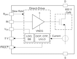
Integrating a GaN FET, a driver, and protection circuitry into a single package is another option. The LMG341xR070 (Fig. 10) provides an alternative to cascode GaNs or standalone devices with separate drivers. The device’s gate driver enables 100-V/ns switching with near-zero VDS ringing; current-limiting circuitry protects against unintended shoot-through events. Overtemperature shutdown prevents thermal runaway, and system interface signals provide self-monitoring capability.
10. The LMG341xR070 combines a 600-V GaN FET with a driver and protection circuitry. (Source: TI Products: LMG3410R0710)
Resources
Texas Instruments has multiple resources to help engineers add GaN devices in their designs. The GaN overview page is a good place to start; it contains GaN-related white papers, application notes, product pages, and reference designs.
We discussed the operation of the ACF in this April 2018 article. Pei-Hsin Liu’s paper at the 2018 Texas Instruments Power Supply Design Seminar also reviews ACF operation in great detail. The seminar includes a set of training videos on the same topics, too. For another example of GaN-related improvements, consult this series of videos on resonant converter topologies.
Sponsored Resources:

