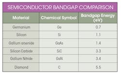
A key semiconductor characteristic is bandgap that indicates the amount of energy required to jolt an electron into a conducting state. A wide bandgap (WBG) enables higher-power, higher switching-speed transistors. WBG devices include gallium nitride (GaN) and silicon carbide (SiC), which are listed in the table along with other semiconductors.
WBG benefits include:
- Elimination of up to 90% of the power losses that occur during power conversion.
- Up to 10X higher switching frequencies than Si-based devices.
- Operation at higher maximum temperature than Si-based devices.
- Systems with reduced lifecycle energy use.
Although WBG semiconductors now cost more than silicon devices, they may eventually be competitive as manufacturing capabilities improve and market applications grow. Several challenges must be addressed to make WBG materials more cost-effective, including:
- Production of larger-diameter WBG wafers.
- Use of novel designs that exploit the properties of WBG materials.
- Use of alternative packaging that enables higher-temperature WBG devices.
- Design of systems that integrate WBG devices so that they take advantage of their unique capabilities.
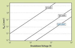
GaN and SiC semiconductor materials allow for smaller, faster, more reliable devices with higher efficiency than their silicon-based cousins. These capabilities make it possible to reduce weight, volume, and lifecycle costs in a wide range of power applications. Figure 1 compares the breakdown voltage and on-resistance of Si, SiC, and GaN devices.
1. Characteristics comparison of Si, SiC, and GaN.
Gallium oxide (GaO) is another semiconductor material with a wide bandgap. GaO has poor thermal conductivity, but its bandgap (about 4.8 eV) exceeds that of SiC, GaN, and Si. However, GaO will need more R&D before becoming a major power-system participant.
SiC
Compared to Si, SiC has:
- On-resistance up to two orders of magnitude lower.
- Reduced power loss in power-conversion systems.
- Higher thermal conductivity, and higher temperature operation capability.
- Enhanced performance due to material advantages inherent in its physical properties.
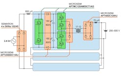
SiC excels over Si as a semiconductor material in 600 V and higher-rated breakdown voltage devices. SiC Schottky diodes at 600- and 1200-V ratings are commercially available and accepted as the best solution for efficiency improvement in power converters. Figure 2 illustrates an example of using SiC devices in an EV battery charger, which was developed at North Carolina State University.
2. SiC power modules and diodes (with “APT” designations) are included in the power stage of a prototype EV battery charger developed at North Carolina State University. Semikron diodes are high-power silicon devices.
A design barrier for SiC is low-level parasitics. If there are too many internal and external parasitics, their performance can decrease to that of a silicon device, or it can cause circuit malfunctions. To break through this barrier, power designers may have to adopt new design and measurement techniques.
Conducted EMI can accompany the fast voltage and current switching transients produced by SiC MOSFETs. Internal and external SiC parasitics are affected by these switching transients and are the primary cause of EMI. System packaging configurations can aid EMI reduction, such as a three-dimensional spatial layout that utilizes multi-layer PCB technology and use of surface-mount technology (SMT) components.
You can also block EMI with barriers of conductive materials. This shielding is typically applied to enclosures to isolate electrical devices from their surroundings, as well as to cables to isolate wires from the environment through which the cable runs.
SiC MOSFETs are available as 1200-V, 20-A devices with a 100-mΩ RDS(ON) at a +15-V gate-source voltage. Besides the inherent reduction in on-resistance, SiC also offers a substantially reduced on-resistance variation over operating temperature. From 25 to 150°C, SiC variations are in the range of 20% versus 200% to 300% for Si. The SiC MOSFET die is capable of operation at junction temperatures greater than 200°C, but are limited by its TO-247 plastic package to 150°C. The technology also benefits from inherently low gate charge, which enables high switching frequencies to be used, allowing for smaller inductors and capacitors.
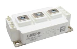
3. Shown is Wolfspeed’s CAS300M17BM2 SiC half-bridge module.
Wolfspeed’s (Cree) CAS300M17BM2 power module includes 1.7-kV, 8.0-mΩ RDS(ON). SiC MOSFETs. This all-SiC Half-Bridge Module (Fig. 3) features:
- Ultra-low loss
- High-frequency operation
- Zero-reverse-recovery current diode
- Zero turn-off tail current MOSFET
- Normally-off, fail-safe operation
- Ease of paralleling
- Copper baseplate and aluminum-nitride insulator
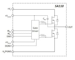
Apex Microtechnology’s SA110 (Fig. 4) is a fully integrated half-bridge SiC power module. It provides up to 20-A continuous output and can operate at over 250-kHz speeds. Its protection features include undervoltage lockout (UVLO) and active Miller clamping.
4. Apex Microtechnology’s SA110 SiC power module can operate with a 450-V supply.
Gate driver ICs suitable for SiC MOSFETs are available from:
- Texas Instruments’ UCC2753x IC family of single-channel, high-speed gate drivers capable of driving SiC MOSFET power switches by up to 2.5 A source and 5 A sink (asymmetrical drive) peak.
- IXYS’ IXD_609SI is an automotive-grade, high-speed gate driver. Its output can source and sink 9 A of peak t, while producing rise and fall times of less than 45 ns. Both the output and input are rated to 35 V. It’s AEC Q100-qualified and available in an 8-pin Power SOIC package with an exposed metal back.
- Avago’s (Broadcom) ACPL-P346 is a high-speed 2.5-A gate drive optocoupler that contains an AlGaAs LED, which is optically coupled to an integrated circuit with a power output stage. This optocoupler is ideally suited for driving power and SiC MOSFETs used in inverter or ac-dc/dc-dc converter applications.
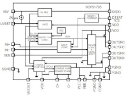
- ON Semiconductor’s NCP51705 is a SiC gate driver (Fig. 5) that includes VDD positive supply voltage up to 28 V; high peak output of 6 A source and 10 A sink; separate signal and power ground connections; separate source and sink output pins; internal thermal-shutdown protection; and separate non-inverting and inverting TTL, PWM inputs.
5. ON Semiconductor’s NCP51705 SiC gate driver.
Gate-Drive Layout
For fast switching, the gate-drive interconnections must have minimum parasitics, especially inductance, therefore:
- Locate the gate driver as close as possible to the SiC MOSFET.
- Exercise care selecting an appropriate external gate resistor to manage voltage overshoot and ringing.
- Use ferrite beads to minimize ringing while maintaining fast switching speed.
- Use a high-value resistor (10 kΩ) between gate and source to prevent excessive floating of the gate during system power-up propagation delays.
GaN
The temperature coefficient of a GaN FET’s on-resistance is positive like the silicon MOSFET, but the magnitude is significantly less. Compared to a silicon semiconductor, GaN’s higher electron mobility enables a smaller-size device for a given on-resistance and breakdown voltage. As a result, GaN devices can be physically smaller and have electrical terminals closer together for a given breakdown voltage requirement.
Silicon power MOSFETs have not been able to keep pace with the changes in power electronics applications. Many applications have reached the silicon MOSFET’s theoretical performance limit, so they must turn to another semiconductor material, such as GaN.
The threshold of enhancement-mode GaN FETs is lower than that of silicon MOSFETs. This is made possible by the almost flat relationship between threshold and temperature along with the very low gate-to-drain capacitance (CGD). The device starts to conduct significant current at 1.6 V, so care must be taken to ensure a low impedance path from gate-to-source when the device needs to be held off during high-speed switching.
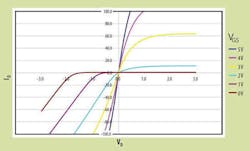
6. Depletion-mode GaN characteristics.
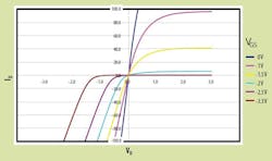
7. Enhancement-mode GaN characteristics.
GaN transistors may be depletion or enhancement mode. The depletion-mode transistor is normally on and is turned off with a negative voltage relative to the drain and source electrodes (Fig. 6). In contrast, the enhancement-mode transistor is normally off and is turned on by positive voltage applied to the gate (Fig. 7). Depletion-mode transistors are inconvenient because at startup of a power converter, a negative bias must first be applied to the power devices or a short circuit will result. Enhancement-mode devices don’t have this problem: With zero bias on the gate, an enhancement-mode device is off and will not conduct current.
Initially, GaN-on-silicon transistors were depletion-mode types. They operated like a normally on power switch that required a negative voltage to turn them off. However, the ideal mode for designers is an enhancement-mode transistor that’s normally non-conducting and requires a positive voltage to turn it on. Efficient Power Conversion (EPC) produces an enhancement-mode, eGaN, transistor using a proprietary process with a GaN-on-silicon structure. In operation, a positive gate voltage turns the enhancement-mode GaN transistor on.
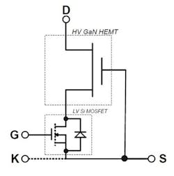
Transphorm employs a cascode configuration with a depletion mode GaN (Fig. 8). This provides the ruggedness of a silicon gate, coupled with the improved voltage-blocking characteristics of a high-voltage GaN. There are no special requirements for the gate driver since the gate is connected to a standard silicon gate rated at ±20 V with a threshold around 2 V.
8. Transphorm’s depletion-mode GaN transistor uses a cascade configuration.
GaN Drivers
Important parameters for driving a GaN FET are:
- Maximum allowable gate voltage
- Gate threshold voltage
- Body diode voltage drop
The maximum allowable gate-source voltage for an eGaN FET of 6V is low compared with traditional silicon. The gate voltage is also low compared to most power MOSFETs, but doesn’t suffer from as strong a negative temperature coefficient. And, the body-diode forward drop can be a volt higher than comparable silicon MOSFETs.
Because the total Miller charge (QGD) is much lower for an eGaN FET than for a similar on-resistance power MOSFET, it’s possible to turn on the device much faster. Too high a dv/dt can reduce efficiency by creating shoot-through during the “hard” switching transition. It would therefore be an advantage to adjust the gate-drive pull-up resistance to minimize transition time without inducing other unwanted loss mechanisms. This also permits adjustment of the switch-node voltage overshoot and ringing for improved EMI.
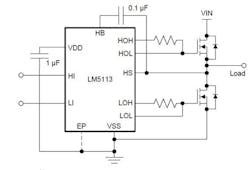
9. The LM5113 half-bridge gate driver targets GaN MOSFETs.
The LM5113, from Texas Instruments, is a half-bridge driver for eGaN FETs that implements bootstrap regulation (Fig. 9). Integrated in the undervoltage lockout is an overvoltage clamp that limits bootstrap voltage to 5.2 V, ensuring sufficient reliable operation under all circuit conditions. Besides the clamp, there are separate source and sink pins, >50 V/ns dv/dt capability, matched propagation time, 0.5-Ω pull down, and separate high-side and low-side inputs that improve efficiencies.
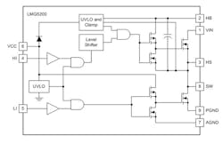
10. Texas Instruments’ LMG5200 GaN half-bridge power stage.
Texas Instruments’ LMG5200 is an 80-V, 10-A driver plus GaN half-bridge power stage using enhancement-mode GaN FETs (Fig. 10). It consists of two 80-V GaN FETs driven by one high-frequency GaN FET driver in a half-bridge configuration. Features include:
- Integrated 15-mΩ GaN FETs and driver
- 80-V continuous, 100-V pulsed voltage rating
- Package optimized for easy PCB layout, eliminating the need for underfill, creepage, and clearance requirements
- Very low common source inductance to ensure high slew-rate switching without causing excessive ringing in hard-switched applications
Virtually all commercially available GaN power semiconductors are now lateral devices that can’t handle over about 600 V. New research is focused on producing a vertical GaN structure that’s better for medium- and high-power applications. These are devices where the current, instead of flowing through the surface of the semiconductor, flows through the wafer, across the semiconductor.
Vertical devices are better in terms of how much voltage they can manage and how much current they control. Current flows into one surface of a vertical device and out the other. That means that there’s simply more space in which to attach input and output wires, which enables higher current loads. Advantages of vertical GaN FETs could include:
- Device dimensions (and cost) roughly independent of breakdown voltage
- Vertical current extraction >100 A possible
- Uniform heat generation and dissipation
- Reduced dynamic on-resistance and current collapse
- New flexibility for normally-off device technology
- Ultra-low leakage current
- Potentially better reliability as E-field far from surface
- Avalanche breakdown demonstrated
- Drift region could be graded for optimum critical field

