Download this article in PDF format.
According to industry research firm Yole Développement, electronics manufacturing is growing at a steady rate above U.S. GDP in part due to power electronics (Fig. 1). Power devices have found their way into high-value products across different market segments such as information technology, electric motor drives, grid infrastructure, automotive, and aerospace. While the first three are mature markets, electric aerospace and automotive are developing.
1. The market for power devices continues to expand and grow.
For the power-generation industry, advances in power devices is continuing to drive efficient and reliable power-grid infrastructure. Currently, up to 40% of generated electric power passes through power electronics between generation and end use. As the power consumption of data-center applications grows in relation to the total electrical power consumption, data-center architectures rely on high-efficiency designs. Innovations in power electronics drive more electric aerospace applications such as no hydraulic networks with more or full electric engines.
In electric vehicles, power devices are used in energy storage, electric drive and power conversion, interior, thermal, powertrain, and chassis. Electric-vehicle adoption presents a high-volume opportunity for power electronics. It’s expected to grow to a $3B market by 2022.
The two major technologies that drive the growth are SiC (silicon carbide) and GaN (gallium nitride) thanks to superior material properties. SiC is typically used in high power applications (10 kV and beyond) and have the benefits of lower switching losses and lower cost, but with less reliability. GaN is usually employed in high-speed applications (higher switching frequencies). Other advantages are high operating temperatures, high breakdown voltage, and being more robust, reliable, and rad-hard. However, it has the disadvantage of material mismatch (GaN on Si or SiC) and higher cost. The table provides a summary of key material properties.
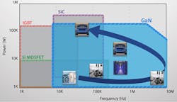
SiC and GaN technologies have found their space in the applications as shown in Figure 2.
2. Wide-bandgap semiconductors will find homes in an array of applications. (Source: GaN Systems, Styles)
Manufacturing Challenges
Due to limited market volume until recently, there hasn’t been much advancement in manufacturing in this space. The industry was able to meet the demand mostly on 2- and 4-in. wafer diameter processes until the end of the last decade. Industry adopted 6-in. wafers a couple of years back and the limited volume of production using 8-in. wafer process is a sign that demand is picking up.
However, it pales in comparison to the digital logic industry, which has migrated to a 12-in. wafer process a long time ago. Obviously, there’s supply where there’s demand. Market adoption of power devices driven by evolving applications and maturity in manufacturing (in terms of cost and defect reduction) are going to be the main growth drivers for years to come.
Let’s look at one of the major aspects that involves the so-called extrinsic defects originating mainly from the manufacturing process itself. One of the important processing steps when it comes to the origination of a defect is epitaxial deposition. Bulk drift layers are formed using this step. It’s a long processing step that needs to have high purity, but it has a high propensity to generate more defects.
Another subsequent yet critical step is the so-called ion implantation, where the appropriate dopants are added to the bulk layer. The process variation needs to be tightly controlled across the wafer and between the wafer and lots to achieve uniform thickness. Variation outside the tolerance significantly alters the device characteristics.
Device performance metrics such as breakdown voltage, which is indicative of blocking voltage across the device, are determined by the quality of the process in the form of thickness and doping uniformity. Higher defect density in gate oxides can be a limiting factor for failure mechanisms such as time-dependent dielectric breakdown (TDDB).
Advances in manufacturing techniques will play a key role in not only enabling high-volume production capabilities, but delivering a quality product to the market as well.
Advantages of Wide-Bandgap Devices
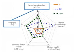
The most telling graphic that sums up the advantages of the wide-bandgap device compared to its silicon counterpart is the famous web graph shown in Figure 3. As shown, the large bandgap and the critical electric field enable high voltages to be blocked with thin layers, resulting in lower resistance and associated conduction losses. Thin layers not only provide low on-resistance, but allow for smaller form factors and reduced capacitance, leading to higher frequency operation.
3. Wide-bandgap semiconductors offer a number of advantages over silicon. (Source: PowerAmerica, Veliadis)
Large bandgap also produces low intrinsic carrier concentration, resulting in low leakage and high temperature operation. Large thermal conductivity is a key benefit for high power operation with limited cooling requirements.
Device Types
There are numerous device structures; each type is unique and is used to address specific needs. For SiC technology, the criteria all device types try to achieve is lower on-state resistance (RDS(ON)) and high breakdown voltage (VBR). Lateral devices have been commonplace, but they have the limitation of large areas required for blocking voltage. SiC devices with blocking voltages up to +900 V are typically of vertical configuration.
Multiple device types are fabricated in SiC technology. Unipolar devices are those where conduction is by one carrier type such as an electron. Some of the unipolar devices are MOSFET, JFET, and junction barrier Schottky diode. These have higher conduction losses but faster switching. Some of the bipolar devices are BJT, thyristor, ISBT, and PIN diode. They have lower conduction losses due to both electrons and holes as charge carriers, but they utilize slower switching with higher losses.
Due to its superior properties, the high electron mobility transistor (HEMT) is a device structure commonly used with GaN technology. It’s purely of the lateral type and the device operates in both depletion mode and enhancement mode. Depletion mode is normally on and can be turned off with negative voltage. Enhancement mode is normally off and turned on by the application of a positive voltage at the gate. It has lower conduction losses (RDS(ON)) with faster switching speed as shown in Figure 2. There are no losses associated with this device type due to ringing or EMI effects thanks to the absence of body-diode operation.
Reliability
Wide-bandgap devices are susceptible to different failure mechanisms, some of which are common to silicon devices. Due to the high blocking voltage for these devices, the following breakdown phenomena are possible: gate-oxide breakdown, SiC breakdown, edge-termination breakdown, threshold voltage drift over time, or reduction in current flow due to increase in resistance.
There’s a need for high electric-field reliability due to high blocking voltage. Accelerated lifetime tests such as HTOL, HTGB, HTRB (high-temperature operating life, gate bias, and reverse bias, respectively) are performed to screen parts that are marginal prior to shipping. However, for certain device types, they don’t completely capture or characterize the intrinsic wearout and aging failure mechanisms like dielectric breakdown (TDDB) or bias temperature instability (BTI).
Dielectric breakdown occurs when there’s a formation of interface and bulk traps due to high electric field, eventually resulting in a short. Depending on the device types and materials used, other failures like avalanche breakdown could occur at test voltages before the occurrence of intrinsic reliability mechanisms.
Threshold voltage stability (P or NBTI, depending on the polarity of applied bias) is another important intrinsic reliability mechanism that causes the gradual shift in device threshold voltage (VTH) over time, affecting the on-state and blocking characteristics. GaN devices are susceptible to dielectric breakdown in the gate dielectric during forward bias and near the field plate and gate corners during off state.
Depending on the application, there’s a third-quadrant operation of power devices that can’t be ignored. Reliability of the body diode is typically stressed in the HTOL tests, but the failure mechanisms corresponding to such operation aren’t completely characterized. Product qualification, depending on the market it serves, requires performing standard tests to demonstrate zero failures with industry-standard models and parameters (for example, 0.7-eV activation energy). They’re not test-to-fail type tests based on a mission profile, which brings out the true performance characteristics and reliability of the devices.
Wide-bandgap devices are susceptible to terrestrial neutrons. When a device gets impacted with a neutron particle, it has the propensity to collide with lattice atoms, creating an ionization path in the trajectory. This results in large current transients leading to gate burn out. This is a parasitic bipolar turn-on effect or gate rupture that’s a gate-oxide failure.
Some reliability issues crop up with packaging. Silicon packaging technology isn’t enough for wide-bandgap devices. To minimize thermal resistance and thermo-mechanical stresses generated due to high power dissipation, double-sided cooling is often required. Wire-bond techniques typically employed for low-voltage logic devices are to be replaced with planar interconnects using topside copper tabs soldered to die. Encapsulation material ought to have required dielectric strength to meet the high operating voltage and temperature of the die. Finally, the die attachment and interface material must have a high melting point with good thermal conductivity.
Standard qualification doesn’t suggest the part can meet a desired lifetime nor that it has lower defectivity. Demanding an often-different mission profile than what’s been tested could produce field acceleration and failure modes that haven’t been screened by standard tests. The reliability challenges must be addressed with the right software analysis tools and techniques prior to product or system design to prevent expensive field failures.
Emerging Technology
Ongoing research in the field of emerging technology is focused on bringing ultra-wide-band devices to market. Materials such as diamond and aluminum nitride (AIN) have much higher breakdown field strength compared to existing material types Si, SiC, GaAs, or GaN, but they have limited practical applications.
Ultra-wide-bandgap materials in the range of 4.5 to 5.0 eV aim to push the breakdown strength much higher without compromising other critical properties such as electron mobility and thermal conductivity. More device structure optimization is required to obtain the desired performance metrics to satisfactory levels.
Challenges and Future Opportunities
As the market requirements for evolving market segments such as automotive, electric aerospace, and data-center applications gets more stringent than traditional markets, wide-bandgap device capabilities have to increase to demonstrate a high junction temperature (175 to 200°C) range of operation for higher-quality-grade products, a target of 0 PPM, demonstrate significantly higher field hours, and a more in-depth understanding of failure modes related to die, package, and system levels.
As emerging applications start to drive growth and define the requirements, opportunities will present itself for advances in manufacturing and device design to enable higher volume with better quality, reliability, and reduced cost.
Ashok Alagappan is a Lead Consulting Engineer with ANSYS.


