>> Electronic Design Resources
.. >> Library: Article Series
.. .. >> Article Series: PowerBites
What you'll learn:
- Novel wireless charging solutions can charge multiple types of robots from the same transmitter.
- New GaN FET family enhances switching figures of merit and on-state performance for automotive, 5G apps.
- Microchip’s latest 3-kW TVS vertical arrays built for aviation and space systems plus other harsh environments.
Autonomous Wireless Charging for Happier, More Productive Robot Fleets
As fleets of robots grow increasingly common throughout the logistic, delivery, and inspection industries, keeping them properly charged has remained a challenge. That’s mostly due to conventional charging systems' requirements for a physical electrical connection, and some level of human intervention.
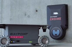
These bottlenecks have been eliminated by a solution developed by WiBotic, with the assistance of Vicor. WiBotic's wireless charging solutions facilitate “many-to-many” operation, in which multiple types of robots (even from different manufacturers) can charge from the same transmitter at different times. To support these heterogeneous fleets, their transmitters are able to adjust their outputs to accommodate a wide range of battery chemistries, voltages, and charging currents.
WiBotic's wireless charging solution required a very efficient, cool-running power supply that was reliable enough to support continuous unattended operation. This role was filled by the Vicor 48-V VI Chip PRM Regulator, a 400-W high-efficiency converter that operates from a 36- to 75-V input. The device powers the adaptive matching transmitter onboard the WiBotic TR-110 wireless charging station, which feeds power wirelessly to the robot’s or UV’s onboard receiver.
The PRM accepts 48 V from an ac-dc power supply and the output voltage is adaptively controlled and trimmed from approximately 20 to 55 V. The Vicor PRM enables consistent, high-efficiency conversion across the full range of impedances, flexibly supporting “full charge” and “trickle charge” modes with no significant drop-off in efficiency at lower power levels.
Click here to learn more about the WiBotic wireless charging application.
Next-Gen 650-V GaN Devices with Advanced Thermal Management Target Automotive, 5G, and Data-Center Apps
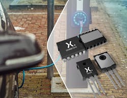
Nexperia announced a new family of gallium-nitride (GaN) FET devices, fabricated in its advanced high-voltage GaN HEMT H2 process, which enables superior switching figures of merit (FOMs) and on-state performance with improved stability. The devices also simplify application designs, thanks to their cascode configuration that eliminates the need for complicated drivers and controls.
The new GaN process employs through-epi vias, which reduces defects and shrinks die size by around 24%. When initially offered in a traditional TO-247 package, its RDS(on) will shrink to just 41-mΩ (max., 35 mΩ typ. at 25 °C) high threshold voltage and low diode forward voltage. The new devices' performance will improve further when they become available in the company’s proprietary CCPAK surface-mount packaging. In this configuration, they will offer even lower RDS(on)—39 mΩ (max., 33 mΩ typ. At 25 °C)—as well significantly better thermal performance.
Because the parts are configured as cascode devices, they’re also simple to drive using standard Si MOSFET drivers. In addition to providing the efficiency and reliability to telecom, server-farm, and data-center applications, both packaging options will meet the requirements of the AEC-Q101 standard for automotive applications in 2021.
Nexperia's 650-V GAN041-650WSB in the TO-247 and GAN039-650NBB in the CCPAK are sampling now. More information, including product specs and datasheets, is available here.
PowerBites Says:
Although the big news in this story is the advanced GaN process, advanced packaging comes in a close second. For most of us EEs, device packaging is a boring, unglamorous issue that can be ignored or left to others. But we ignore it at our own peril as the power densities of the stuff we design continue to climb. Fortunately, power-smart companies like Nexperia have been paying close attention to it, in this case, for a couple of decades.
In a nutshell, its proprietary CCPAK1212 package uses what the company refers to as "copper-clip SMD packaging" to virtually envelop the chip thick copper leads that serve as both thermal paths and electrical paths. In addition to providing a very low-resistance thermal path ( typ. <0.5 K/W), Nexperia claims that the package dramatically reduces parasitic inductances. I apologize for forgetting to ask if the 3X reduction is in comparison to traditional TO-247 packages, or some other device. I also regret that I neglected to get a graphic that shows the unique features of the CCPAK1212 housing, but I'll do better next time.
Surge Busters! 3-kW TVS Diode Arrays Built for Harsh Environments
Microchip's portfolio of transient-voltage-suppressor (TVS) vertical arrays – the MDA3KP TVS—has been expanded to provide more solutions for critical applications, such as aviation and space systems that rely on digital and logic functionality as well as circuitry in engine control units, environmental controls, instruments, and actuators. The 3-kW-rated family of devices includes more than 25 products with different screening levels, polarities, and qualification standards. It’s also intended for data centers, the 5G infrastructure, and other communication systems that rely on complex circuitry requiring protection.
The company’s MDA3KP TVS family of integrated fast-reacting avalanche-breakdown-diode (ABD) arrays offers a wide range of devices and operating voltages, all tested and qualified to to a high standard based on the MIL-PRF-19500 JANTX level equivalence standard. They have also been exposed to various levels of testing to ensure that they meet the aircraft lightning protection requirements set forth in the standard for environmental testing of avionics, RTCA DO-160G (Lightning Induced Transient Susceptibility).
Available in unidirectional and bidirectional construction in standoff voltages of 6 to 40 V, the components provide electrostatic discharge (ESD) and electrical fast transients (EFT) protection according IEC standards, and maintain a peak pulse power rating of 3000 W at 10/1000 µs. With an extended temperature range from −55 to +150°C, the devices are lot traceable, surge tested, and have a moisture sensitivity level (MSL) of Level 1, demonstrating that these devices are ready for use in harsh environments.
For additional information, visit http://www.microchip.com/design-centers/power-management/transient-voltage-suppressors.
Are Quantum-Tunnel Transistors Real, and What Do They Mean for Power Technology?
It's tough to take the audacious claims being made by Search For The Next (SFN), a Nottingham, England-based technology startup, seriously because, if they are true, they will force the entire semiconductor industry to question the assumptions on which we've based nearly everything for the past 50+ years. Then again, after even a brief introduction to their research, and how they tend to apply it, it's even tougher to ignore their claims.
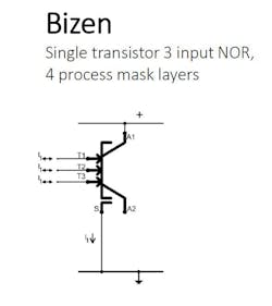
SFN says its new process, which they refer to as "Bizen,” is based on the principles of quantum-tunnel mechanics and can be used to dramatically improve the performance and producibility of any digital or analog semiconductor device. Among other things, making Bizen devices requires just half the process layers, which cuts the time it takes to process a typical wafer full of CMOS devices from 15 weeks to just three.
In addition, SFN claims that the new process achieves a three-fold increase in gate density that produces a matching three-fold reduction in die size. In a recent announcement, SFN said that it has been working been in collaboration with Semefab, a privately-owned semiconductor and MEMS fab based in Glenrothes, Scotland, since 2017 on process development and qualification that should lead to device production in the near future.
To learn a little more about Bizen technology, and how it may affect the electronics industry, check out the full report on Electronic Design.


