Understanding Common Isolated Power ICs for Digital Isolation Systems
This article is part of TechXchange: Exploring Digital Isolator Technology
Members can download this article in PDF format.
What you’ll learn:
- The need for an isolated power supply.
- Different ways to approach designing digital isolation systems.
- The benefits and design considerations of different topologies.
A high-voltage circuit design requires isolation to protect human operators, enable communication to lower-voltage circuitry, and eliminate unwanted noise within the system. Digital isolators offer a simple and reliable path toward achieving high-voltage isolated communication in industrial and automotive applications.
Maintaining the integrity of a signal across an isolation barrier requires the isolation of all coupling paths between the primary and secondary sides of the circuit, including the power supplies. While a digital isolator’s secondary side typically requires little power, system designers often include an additional power allowance to supply power for multiple devices.
Many options are available when designing an isolated power supply for digitally isolated circuits. This article will introduce some of the most popular topologies—flyback, half-bridge (H-bridge) inductor-inductor-capacitor (LLC), push-pull, and integrated isolated data and power solutions—along with design considerations. But first, let’s address the need for isolated power.
Isolating Power for Digital Isolators
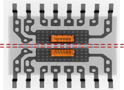
The internal architecture of a digital isolator consists of two separate digital integrated circuits (ICs) on a split leadframe with a high-voltage isolation dielectric barrier between them (Fig. 1). Each IC requires a separate power supply and ground for both the primary and secondary sides of the device, with no physical connection between them. This need is independent of whether a device supports basic or reinforced isolation, and it applies to digital isolators as well as isolated devices with integrated interfaces.
What Are the Power Requirements for a Digital Isolator?
Before selecting a power topology for a digital isolator solution, you will need to determine the basic requirements of the supply, including the input voltage range, output voltage, output power needed for the secondary side, and the number of output rails. Among other considerations for isolated power solutions compared to non-isolated power solutions are system insulation ratings and required creepage and clearance distances, along with electromagnetic-compatibility requirements such asThe input and output signal voltages of a digital isolator often depend on their applied power-supply voltage, and they usually have a direct relationship to the supply voltage (VCC) on the secondary side. Be sure to review the digital isolator datasheet carefully for power-supply requirements before finalizing supply input and output requirements and optimize the output of the digital isolator for the logic levels of interfacing components.
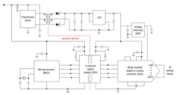
For example, when powering a digital isolator with 5 V that interfaces to a microcontroller, select signals that also are operating at or close to 5-V logic levels on the secondary side (Fig. 2).
Does a Secondary-Side Supply Work for Isolated Power?
In some cases, two separate power-supply rails may already be available within the system for primary- and secondary-side power, as long as you can meet some minimal requirements of the isolator logic. These include power-supply voltage levels matching the input- and output-signal levels, each offering a separate ground.
While the use of existing secondary supplies is an option, noise coupling and supply regulation often become an issue. Designers usually elect to design isolated supplies that are optimized for logic and system noise performance.
Designing an Isolated Power Supply
Let’s explore the different topologies used to generate an isolated power supply. Each one offers distinct benefits depending on the application.
Flyback power supply
A flyback power supply combines a buck-boost converter and a split inductor to form a transformer. This topology is traditionally used to isolate low-power applications. The transformer facilitates generating multiple output rails, and you can easily modify output voltages by varying the turns ratio to accommodate your design needs.
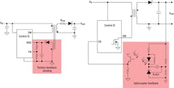
To accurately regulate the output, you need feedback from the secondary side for the pulse-width-modulation (PWM) controller within the buck-boost converter. It’s possible to accomplish this with an optocoupler or an auxiliary or tertiary winding (Fig. 3), which can increase component count and add cost. Furthermore, you must carefully manage the leakage inductance and efficiency of the transformer for regulation, as parasitic capacitance may influence electromagnetic interference (EMI). In general, the flyback topology is a simple, low-cost approach to creating an isolated power supply for digital isolators.
H-bridge LLC power supply
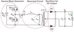
An H-bridge power converter combines a square-wave generator, resonant circuit, and dc output rectifier to supply a secondary-side isolated power output (Fig. 4). The resonant switching circuit is a key component of the design, using two inductors and a capacitor to form the LLC circuit. It regulates the output voltage by changing the frequency of the driving voltage to change the impedance of the resonant circuit.
While this topology offers high efficiency and power density, the circuit’s peak resonance depends on loading conditions. This complicates designs and often requires a pre-regulated input voltage as well as a narrow input and output range to minimize variance.
The H-bridge power converter is traditionally used to isolate medium-power applications, or those that need higher output power. The Power Supply Design Seminar article, “Designing an LLC Resonant Half-Bridge Power Converter,” provides more detail about H-bridge LLC designs.
Push-pull power supply
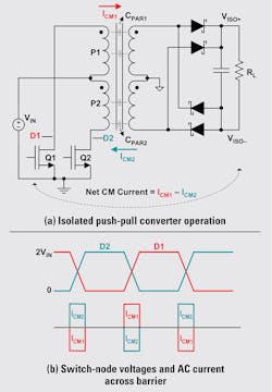
A push-pull converter topology uses electromagnetic induction, or transformer action, to transfer power from the primary side to the secondary side. The circuit employs two identical low-side switches, a center-tapped primary and secondary transformer, and full-bridge rectifier diodes (Fig. 5a). Two switches—Q1 and Q2, operating in alternate cycles—provide the switching for transformer action, which regulates the output voltage in a feed-forward manner, while the transformer turns ratios determines the output voltage.
One benefit of this topology is that the use of center-tapped transformers and identical switches produce a symmetric output profile for current and voltage (Fig. 5b), unlike single-ended flyback topologies or an H-bridge complementary drive topology.
Transformer driver
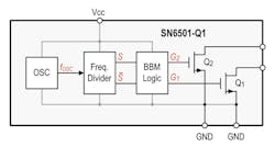
A transformer driver integrates an oscillator and gate-drive circuit, typically with additional features such as overvoltage lockout or slew-rate and duty-cycle control, to simplify push-pull power topology designs. To save space, you can use transformer-driver ICs like the one shown in Figure 6 in place of the switches of the push-pull power topology.
Transformer drivers such as the SN6505B or SN6501 from Texas Instruments (TI) offer a low-noise solution by using low-side switches that are on in alternate clock phases and transfer power continuously across a center-tapped isolation transformer. This continuous power transfer results in much lower peak currents, no dead time, lower emissions, and higher efficiency compared to other topologies.
Such devices can typically be used with a low-dropout regulator (LDO) on the secondary side to regulate the output voltage (Fig. 7), although this addition is optional. To learn more about transformer driver circuit design methodology, see the application note, “Signal and Power Isolation with 3.3 V/5 V Input and 12 V/15 V Output.”
Integrated power-module solutions
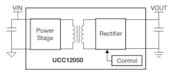
As semiconductor technology advances, the option of integrating EMI-optimized transformers and silicon opens up the possibility of new circuit topologies for powering digital isolator designs. TI’s UCC12050 is an example of an integrated dc-dc bias power supply that provides a single-chip solution for isolating digital isolator power, much like an integrated power module (Fig. 8).
By integrating a power stage and rectifier, the power supply offers a smaller form factor with a significant height and weight reduction compared to discrete solutions. The internal topology control scheme runs closed-loop without an LDO or external feedback components.
Signal isolator with integrated dc-dc converter
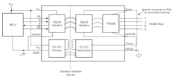
Integrated signal and power ICs combine an isolated dc-dc converter, a transformer, and an LDO with digital isolator signal channels or isolated transceivers in a single package. Data channels are isolated through a dielectric, and chip-scale transformers are used for power isolation, with designs optimized to achieve as small a footprint as possible. Figure 9 shows two examples of integrated solution—one with isolated data and power and the other with an isolated transceiver with isolated power.
Efficiency and emissions are the primary parameters to consider when selecting an integrated power solution. Internal transformer ratios are fixed with integrated designs and typically offer lower output currents, causing efficiency for an integrated solution to be lower than the discrete solution by 20-30%.
Emissions also present a challenge for integrated designs. The use of low-inductance microtransformers requires high-frequency switching, which can result in higher radiated emissions compared to discrete solutions.
For that reason, selecting an integrated solution requires a review of measured emissions performance and an additional focus on board- and system-level techniques to achieve performance targets. Examples include choosing lower supply voltage operation and optimized filtering and layout techniques to obtain the lowest possible radiated emissions at the system level.
Despite the need to optimize your layout at a board and system level, emissions performance for integrated solutions continues to improve with each subsequent generation. Comité International Spécial des Perturbations Radioélectriques (CISPR) 32 is the European emissions standard used to differentiate between Class A and Class B equipment and specifies conducted and radiated emissions for each class.
The ISOW7741 integrated digital isolator with isolated power, ISOW1412 integrated isolated RS-485 transceiver with power, or ISOW1044 isolated controller area network (CAN) transceiver with an integrated dc-dc converter meet CIPSR 32 Class B limits with a significantly smaller solution size than discretely designed alternatives.
Despite some additional design time for optimizing integrated solutions, the elimination of a transformer on the board, reduction in board size, and improved ease of certifications are worthwhile tradeoffs to achieve a high-performance design in the smallest possible footprint. While discrete solutions have the highest efficiency and lowest emissions, integrated solutions save board space and time-to-market.
Read more articles in TechXchange: Exploring Digital Isolator Technology
