A popular power source for portable devices is a single lithium-ion (Li+) cell battery, which provides 4.2 V at full charge and 2.8 V near the end of discharge. Some functions within portable electronics, such as RF amplifier circuits for wireless communication and common microcontrollers, require 2.8- and 3.3-V input power rails.
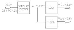
These rails are normally provided by low-noise linear-dropout regulators (LDOs) to ensure a quiet supply. The LDO’s inputs (VCC in Fig. 1) must be at a slightly higher voltage than the highest LDO output. Hence, VCC ends up right in the middle of the Li+ battery’s range of operation. The use of a step-up/down voltage regulator, capable of operating from an input (VBATT) that can be higher or lower than the output, becomes a necessity.
1. The LDO’s inputs must be at a slightly higher voltage than the highest LDO output.
In portable applications, the voltage-regulator efficiency is of the utmost importance since higher efficiency translates into longer untethered operation. This article reviews the available options, compares their performance, and presents a one-two punch approach to the most efficient solution.
Bypass-Boost
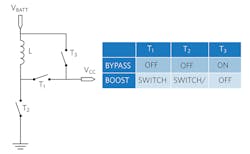
One way to solve the battery-to-LDO voltage mismatch is to use a bypass-boost converter, namely a boost converter with an extra “pass” transistor integrated between the power source (VBATT) and the LDO input (VCC). Figure 2 shows the bypass-boost powertrain architecture and its operation table. Here, the bypass transistor T3 accomplishes a “poor man’s” step-down operation.
2. The bypass-boost powertrain architecture and its operation table highlight a “poor man’s” step-down operation.
This architecture can only regulate VBATT voltages lower than the set VCC = 3.4 V. For VBATT > 3.4 V, the boost converter stops regulating and the pass transistor turns on, directly connecting VBATT to VCC. For most of the time (VBATT > 3.4 V), the pass transistor in the bypass-boost architecture literally “passes the buck” to the LDOs downstream. The LDOs bear the task of regulating the high VBATT value down to their output set values. Since this regulation is linear, the result is high power dissipation inside the LDO. The higher heat generated becomes a burden on the PCB in terms of cost, size, and reliability.
Buck-Boost
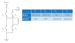
In contrast to the bypass-boost architecture, a buck-boost converter used in this circuit will never stop regulating its output to 3.4 V. In addition, the regulation is entirely switch mode, which provides high-efficiency operation. Figure 3 shows the buck-boost powertrain architecture and its operation table.
3. In contrast to Fig. 2, this uses a buck-boost powertrain.
For VBATT > VCC, the IC regulates in buck (step-down) mode, while for VBATT < VCC, it seamlessly transitions to boost (step-up) operation. This ensures that the VCC output remains in regulation and is glitch-free. The entire battery voltage range is covered in a switch-mode, high-efficiency fashion.
Buck-Boost vs. Bypass-Boost
We compare the system efficiency (from VBATT to VOUT) using Maxim’s MAX77816 buck-boost IC versus a competitive bypass-boost IC (Fig. 4). Each step-up/down converter feeds a single 3.3-V LDO loaded with 500 mA.
4. This efficiency test setup uses a Maxim’s MAX77816 buck-boost IC or a competitive bypass-boost IC for the step up/down block.
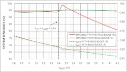
Figure 5 shows the result of the comparison. Solid curves indicate efficiency and dashed curves show battery current consumption for each solution. The buck-boost efficiency (above 93% across the entire operation range) is far superior to that of the bypass-boost (as low as 81% with full battery). This superior performance is due to the ability of the buck-boost IC to supply power to the LDO in switch mode across the entire range of operation. The vertical dotted line highlights the transition point from step-up/down to step-down/up mode.
5. The buck-boost efficiency is above 93% across the entire operation range, making it far superior to that of the bypass-boost.
Buck-Boost vs. Buck-Boost
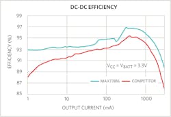
In Figure 6, we compare the efficiency (from VBATT to VCC) of MAX77816 to a similar buck-boost IC. The comparison in this case uses VCC = 3.3 V and VBATT = 3.3 V, since the competing data is readily available, as opposed to VCC = 3.4 V.
6. These results are based on VCC = 3.3 V and VBATT = 3.3 V, since the competing data isn’t available for VCC = 3.4 V.
Test results show that the MAX77816 outperforms the competing buck-boost over the entire current range from 1 mA to 3 A. The efficiency advantage is as high as 5%. This leads to the “first punch” of the solution to the efficiency problem: Use the best available buck-boost converter.
DVS for Efficiency
Dynamic voltage scaling (DVS) can further improve system efficiency. The buck-boost load is normally comprised of many LDOs, all at different VOUT. These LDOs may not all be operational at the same time. When the LDO with the highest VOUT is disabled, the system can lower the buck-boost output (VCC) in a manner compatible with the next highest VOUT, effectively reducing the voltage dropout and thus saving power.
DVS With Direct Hardware Control
A two-level output voltage selection is easily achieved with a dedicated DVS logic-input pin when direct hardware control is desired. The MAX77816 supports a programmable general-purpose input pin that can be configured as a DVS input between two preset/programmable values. The default values are 3.4 V and 5 V, but can be adjusted upon request. For further power savings, a more granular selection of output voltages must be implemented, which requires a different type of output voltage control. This is discussed in the next section.
The Advantage of an I2C-Driven DVS
The MAX77816 features an I2C-compatible serial interface, used for regulator on/off control, setting output voltage value and slew rates, and additional functions. With I2C, the regulator output voltage can be dynamically adjusted. This, in turn, enables finer control of system power consumption without the need for a dedicated DVS input pin.
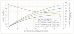
The curves in Figure 7 refer to a Li+ battery-powered, step-up/down converter loaded with a 3-V-output, 32-mA LDO, and a second 2.85-V-output, 18-mA LDO. The descending orange curve is the discharge profile of the Li+ battery with typical system shutdown at 3.4 V (systems seldom deplete the battery all the way down to 2.8 V). The rest of the curves profile the accumulated extended battery operating time of the MAX77816 due to voltage scaling.
7. The descending orange curve is the discharge profile of the Li+ battery with typical system shutdown at 3.4 V. The rest of the curves profile the accumulated extended battery operating time of the system due to voltage scaling.
The light-blue curve shows the advantage of the buck-boost with 3.4-V output versus a boost-bypass architecture. The rest of the curves show the advantage of reducing the buck-boost output VCC via I2C down to 3.15 V for duty cycles from 25% to 75%.
The extended battery operating time varies from 45 to 82 minutes. The second punch of the solution is clear: Employ DVS via an I2C bus.
Conclusion
A comparison of the buck-boost architecture to the bypass-boost architecture shows that, in principle, the buck-boost is a superior architecture. A practical comparison of the MAX77816 buck-boost solution versus a competing bypass-boost solution shows that in operation, the MAX77816 has an efficiency advantage of up to 13%. When compared to a competing buck-boost solution, the MAX77816 outperforms it by as much as 6 efficiency points.
These efficiencies, combined with those derived from dynamic voltage scaling via an I2C bus or via a dedicated DVS input pin, result in extended operation for a battery-powered device of up to 90 minutes. Thus, a buck-boost IC with DVS is the ideal solution for power-stingy portable applications.

