Half-Bridge Flyback Converters Outperform Conventional Types
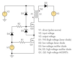
In a half-bridge flyback converter with serially connected MOSFETs, the upper switch pair shares the total voltage in the same way that the low-side switch interrupts input voltage (i.e., the bus voltage) (Fig 2). Meanwhile, the high-side switch interrupts transformer-reflected voltage, along with the voltage spike caused by the transformer’s leakage inductance.
Integrating serially connected switches into the half-bridge flyback helps enhance efficiency because they minimize turn-off losses. This comes in handy for applications dealing with wide input-voltage ranges.
Delving further into this arena, Infineon developed a prototype to study half-bridge flybacks with these serially connected switches. The prototype features an 800-V input/24-V output capable of driving up to 0.33 A.
In looking at applications, the company pinpointed a smart-meter power supply, which requires a converter with low power demands (~8 W) and a wide input-voltage range. A typical flyback topology used in such an application faces limitations arising from MOSFET technology. Foremost among those is the MOSFET’s breakdown voltage, which is on the order of 900 V. As a result, it can’t provide sufficient voltage margin to accommodate transformer-reflected voltage (~200 V) and the peak voltage (~100 V) caused by the transformer’s leakage inductance.
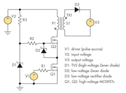
The conventional approach toward designing a reliable switch (i.e., one rated for a VDS of at least 1300 V) demands two MOSFETs connected in series. Such an approach also must incorporate transient voltage suppression (TVS) using a high voltage Zener diode to limit the voltage on low-side switch. That is, when the low-side MOSFET isn’t conducting, transformer current would be directed through the source-gate capacitance of the high-side MOSFET and the TVS diode.
In that situation, two parallel processes are in operation: discharge of the CGS capacitor until the high side MOSFET turns off; and voltage-limiting on the low-side MOSFET, accomplished by turning on the TVS diode. In that situation, the losses in the TVS equal the product of transformer current and TVS voltage.
A half-bridge flyback topology, using a rectifier diode that connects the gate of the high-side MOSFET to the bus (Fig. 2, again), offers a better alternative to the conventional approach. Although the turn-off current discharges the CGS capacitance of the high-side MOSFET, the circuit doesn’t experience any additional losses.
Advantages of the half-bridge flyback include:
• Better efficiency as turn-off switching losses are minimized
• Simple low-voltage drive for high-side MOSFET
• Rectifier diodes can be used instead of a high-voltage TVS Zener diode (D1)
In the conventional solution, prior to turning ON, the MOSFET’s parasitic capacitance would be charged to its breakdown voltage. Taking events in sequence, the switching cycle starts when MOSFET Q1 is turned on by driver V1 (a pulse source).
The next step is to charge the CGS capacitor of the high-side MOSFET using charge from the parasitic capacitance of D1. Once CGS is charged, the high-side MOSFET will turn ON. At that point, the input voltage is applied to the primary side of the transformer, and magnetizing current increases until the low-side MOSFET (Q2) turns off.
In the turn-off sequence, while Q1 is off, the VDS voltage increases until it reaches the breakdown voltage of D1. D1 then starts to conduct, and the low-side MOSFET current (IDS) reroutes to D1 through the CGS capacitance of the high-side MOSFET Q2. The IDS current then discharges CGS and the high-side MOSFET turns OFF. When VDS on Q2 reaches the value of the reflected voltage, diode D3 turns ON, triggering transformer secondary current.
A coarse estimate for driving switching losses (PSW_conv) in this scenario is established with:
PSW_conv = VBR_tvs × (Qg) × fs
where V BR_tvs = breakdown voltage of the TVS Zener diode; QG = gate charge of high-side MOSFET; and fS = switching frequency.
The half-bridge topology’s basic characteristic is that neither one of the two MOSFETs “sees” any voltage larger than bus voltage. That’s why the authors termed this topology the “half-bridge flyback.”
The switching cycle starts when driver V1 (pulse source) turns on Q1. The next step is to charge the CGS capacitor of the high-side MOSFET using the same pulse source V1 and diode D4. When CGS is charged, the HS MOSFET will be turned ON. Input voltage is applied to the primary side of the transformer, and magnetizing current increases until the low-side MOSFET (Q2) is turned off.
In the turn-off sequence, when Q1 is off, VDS voltage increases until it reaches bus voltage V2. The rectifier diode (D5) starts to conduct and the low-side MOSFET current (IDS) then gets rerouted to D5 through the CGS capacitance of Q2. IDS current will discharge the CGS capacitance and the high-side MOSFET will turn OFF. When Q2’s VDS reaches the value of reflected voltage, diode D3 will turn ON and transformer current will start transfer from the primary to secondary side. Losses occur via conduction at D5, in addition to the MOSFET losses.
A coarse estimate of this topology’s switching losses is calculated by:
PSW_hbf = VF × (QG) × fS
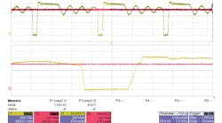
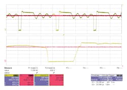
Comparison of the two approaches reveals much smaller losses for the half-bridge flyback topology. (Table 1 and Fig. 3).
The half-bridge flyback converter employs a rectifier diode to limit the low-side MOSFET voltage to bus voltage. This improves efficiency by reducing turn-off loss when the high side MOSFET is turning off.
To simplify the driver stage of converter designs, the half-bridge flyback approach can be extended to forward topologies. A half-bridge forward topology, which will handle magnetizing current much like the half-bridge flyback, will require demagnetizing turns on the forward transformer.
REFERENCES
Ilchmann, Bernd, “Ultra Wide Input Range, HV-BIAS Supply for SMPS with ICE2B265 and SPA02N80,” Published by Infineon Technologies AG, March 2008.
Ivankovic, Mladen, “Half bridge flyback and forward” patent application (Serial No. 13/436,109), March 2012. US 8,653,881 B2, Feb. 18, 2014.
Bjoerk, Fanny; Hancock, Jon; Deboy, Gerald, Application Note: AN-CoolMOS-CP- 01 CoolMOSTM CP- “How to make most beneficial use of the latest generation of super junction technology devices,” published by Infineon Technologies AG, Feb. 2007.
