Apply Pin-in-Paste in Lead-Free PCBs with OSP Surface Finish
This file type includes high-resolution graphics and schematics when applicable.
Dora Yang, Technical Engineer, PCBCart
With improvements in technology enhancing people’s lives, electronic products requirements have become greater in terms of being lighter, thinner, smaller, higher performance, and having more functionality. As a result, overall miniaturization and product integrity are the main focus of development among designers and manufacturers.
To increase the density level of components, lots of single- and double-sided circuit boards primarily manifest surface-mount components (SMCs) or surface-mount devices (SMDs). However, in terms of intrinsic intensity, reliability, and applicability, pin-in-paste (PIP) components in certain cases still hold more advantages than SMCs and SMDs, especially for edge connectors.
For example, in double-sided surface-mount-technology (SMT) boards featuring mixed assembly with a few PIP components on the top, application of PIP technology is helpful to process reduction and cost control. PIP technology is a printing method by template, i.e., some amount of solder paste is printed on the surface of SMCs and on through holes and pads of through-hole mounted components. Upon completion of mounting, soldering is completed after being heated in a high-temperature oven.
PIP technology holds a number of advantages over traditional technology, such as:
• Fabrication and technology process is simplified thanks to the absence of wave soldering.
• Workshop space is saved due to fewer applications of needed equipment, material and workers.
• Production cost is decreased while production cycle is shortened.
• High defect rate caused by wave soldering can be avoided to improve first-pass yield.
• One or more heat-treatment steps can be omitted so that PCB solderability and component reliability will rise.
• Through-hole reflow (THR) technology is able to reduce the amount of flux, avoiding the contamination of flux on PCBs caused by wave soldering.
Properties of OSP Surface Finish
As a transparent organic material surface finish of PCB, on the one hand, organic solderability preservative (OSP) holds an extremely high requirement for PCB storage and short craft time. Meanwhile, usually after one-time high-temperature soldering, the organic protection film on the PCB’s surface will be destroyed so that anti-oxidation capacity will be lost, easily leading to difficulties of second-time reflow soldering.
On the other hand, the flow of solder paste on PCBs with OSP surface finish is worse, and copper tends to be exposed on solder joints, which influences reliability of solder joints. In addition, the appearance of tin coating fails to comply with IPC3 standard. Therefore, generally, PCBs with OSP surface finish are seldom applied in products with PIP technology. Nevertheless, most companies still prefer using PCBs with OSP surface finish because boards have excellent evenness. Moreover, PCBs with OSP hold relatively stable fabrication technology at low cost, which typically isn’t the case for other types of surface finish.
Requirement on Components
Components should adhere to the requirement of reflow in terms of temperature withstanding capacity.
For instance, lead-free process components should withstand be able to withstand temperatures above 260°C for more than 10 seconds. Professional PCB manufacturers should have the capabilities to process a lead-free surface finish. One example is PCBCart, a custom PCB manufacturing and assembly service provider from China, which offers high-end lead-free processing. For experimental purposes, we’ll only apply lead-free craft in this article.
Tin paste is required to be coated on top of vias for THR.
To make this process applicable with PIP technology, the distance between components and board should be in the range from 0.3 to 0.7mm. Under the same conditions (printing parameter, pad and aperture diameter design etc.), pins of PCB components with immersion gold and other types of surface finish is 1.5 mm thicker than the board’s thickness, and the tin coating of solder joints at the bottom is able to meet the requirement of IPC3. However, copper leakage tends to occur with solder joints on PCBs with OSP, thus failing to comply with IPC3 standard.
1. Shown are the basic design requirements for component pins.
After going through the verification process multiple times, tin coating is more effective when pins of components on a PCB with OSP are longer than the thickness of the board by 0.5 to 1.0 mm (Fig. 1).
To stop a component pin from pushing out tin paste inside an aperture, with an insufficient amount of tin inside the aperture, sharp corner or cone processing must be carried out on component pins.
The component-material package requirement should be the same as that of SMT.
Components must adhere to the requirement of automatic mounting of SMT equipment. The requirement covers aspects of component height, component shape, spacing between component pins, etc.
Requirement on Pad Design
PIP technology is applied on PCBs with OSP, but the component layout requirement should be largely compatible with PCBs that have other types of surface finish. The general principle is that small components are placed on one side (bottom side), and large components are placed on the other side (top side) in accordance with the requirement of double-side reflow soldering. Components should not be placed within 2 mm around PIP components. If multiple PIP components exist, the distance between adjacent PIP components should be at least 10 mm to stop the interference caused in the process of automatic mounting.
2. Illustrated are the basic design requirements for through holes and pins.
To avoid generating a tin connection between adjacent pins or between pads (potentially leading to insufficient tin inside an aperture or short circuit), the distance between two adjacent through-hole centers should be at least 2 mm; distance between edges of adjacent pads should be at least 0.6 mm; and distance between the pad edge and aperture diameter should be at least 0.3 mm. Pad aperture diameter is suggested to be larger than component pin diameter by 0.2 to 0.4 mm.
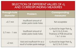
Figure 2 shows the design requirement of through holes and pins: d = diagonal diameter of the square pin, di = diameter of the through hole, and dA = external diameter of through hole. Because PCBs with OSP feature a smaller craft window than those with other types of surface finish, whereby solder joints often experience copper leakage in reflow, diameter of through holes have to be reasonably designed. The table below displays selections of di, illustrating problems and measures to be taken.
Requirement on Stencil Opening Design
The key to the success of PIP technology lies in the accurate calculation of the required amount of tin paste for printing. The volume of alloy required by solder joints can determine the amount of tin paste based on lead shape, diameter of through holes, and thickness of substrate. Calculation of tin-paste volume starts with the application of an ideal solid metal solder joint that completely fills an electroplated through hole, and soldering fillets stay at the top and bottom surface of PCB.
Due to the difference in solder joints with the application of PIP technology, the amount of tin paste required by solder joints is larger than that required by SMT components. Generally, solder in printing tin paste only accounts for approximately 50% of the volume; the remainder is solder flux that will be volatilized with the completion of soldering. As a result, the volume of solder paste will shrink by 50%
To achieve the desired soldering effect, an appropriate amount of tin paste should be maintained on each through-hole pad of through-hole mounted components to supplement the solder. Otherwise, it will cause defects such as an insufficient amount of tin inside the through hole, a void, or bubbles.
With the template thickness and opening size unchanged, solving the problems of insufficient amount of tin for PCBs with OSP, copper leakage, and bad wetting requires application of pre-tin coating at the bottom side (Fig. 3). In addition, a ladder stencil ranging in size from 0.13/0.18 to 0.25 mm is applied at the surface side (Fig. 4).
4. A ladder stencil is applied to the surface side of a PCB.
Other Technology Requirements
Printing parameters
To some extent, printing parameters will affect the filling amount of tin paste in through holes. Tin-paste printing parameters primarily include squeegee pressure, printing speed, separation speed, angle between squeegee and stencil, and stencil cleaning mode and cleaning frequency.
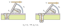
Squeegee pressure and printing speed influence printing quality—if the pressure is too large and/or too high speed, it could lead to insufficient tin amount. Separation speed influences the definition of the tin-paste edge after printing; the printing angle will affect the amount of tin paste filled in the through holes. With other variables unchanged, decreasing the printing angle can increase the tin-paste filling amount (Fig. 5).
5. The diagram shows the relationship between the printing angle and the tin-paste filling amount.
For PCBs with OSP, a tin-paste filling of more than 90% will ensure an excellent soldering effect. The ideal tin-paste filling amount in through holes is when the tin is higher than the bottom pad by 0.5 to 1 mm. If no components with fine spacing are placed around PIP technology components, a squeegee of 45 degrees is initially selected.
Mounting technology
Unlike the SMT of ordinary components, components with PIP technology have a special appearance, as well as greater height and weight, which leads to wide mounting processing capacity for SMD such as accurate mounting positioning and image-processing capacity. PCBs with OSP manifest higher requirements in terms of mounting accuracy to ensure the stability of each mounting. If the requirements aren’t met, problems such as bad mounting and insufficient tin will ensue.
Oven temperature setting
Thermal transmission styles of reflow soldering technology are primarily infrared radiation, hot air convection, and a combination of infrared and hot air. Correctly setting the reflow soldering temperature curves helps guarantee high soldering quality of solder joints.
The setting method of reflow soldering temperature curves for PIP technology is based on tin paste, PCB material, heat-sensitive components, and thermal performance parameters of valuable components. Through practical measurement, it’s been found that a temperature difference of 3 to 5 degrees occurs between the bottom solder joints and component surface of PIP components.
Too much soldering tin inside through holes, as well as the size of these types of components, requires more heat energy, which leads to a relatively slow temperature rise of the solder joints at the bottom of component and inside the through holes. If pre-tin coating method is applied at the bottom of PCBs with OSP, the liquidus temperature (the temperature above which a material is completely liquid) will rise a little in the second reflow soldering. By applying different temperature zones in the reflow oven, temperature in the lower temperature zone can be suitably increased within the window of allowable processing, resulting in a better soldering effect.
Quality testing and judgment standard of solder joints
Quality testing for solder joints of PIP components is different from ordinary SMT components. It’s primarily a two-fold process: filling degree of through holes and wettability outside the solder-ball area. The lowest standard for peripheral wettability of solder is to simply examine both the solder ball and peripheral wetting. Solder joints of pins at the bottom side can be checked by examining their appearance. Ideally, solder joints should appear satiated and be clean around solder joints, without tin balls or flux contaminant. X-ray inspection can be used for testing of pins and through-hole solder joints buried under components.
Dora Yang, a technical engineer for PCBCart.com since 2010, specializes in electronic design, PCB manufacturing, surface finish and substrate material. She obtained her Bachelor's degree from China University of Petroleum and a Master's from Zhejiang University. Although she has worked on present position for only six years, Dora took time on electronics design study, especially PCB design research. She has written a large number of technical articles based on her research, most of which are published on PCBCart.com. If you have any questions related to PCBs or electronic design, feel free to discuss with Dora on Twitter @dorayang0227.


