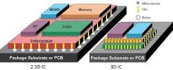
As the semiconductor industry strives to pack more functionality into smaller spaces, 2.5D and 3D integrated circuits (3D ICs) have emerged as a transformative technology. 2.5D layouts connect multiple die on an interposer; 3D IC designs stack multiple layers of chiplets, potentially from different process nodes, into a single, cohesive package (Figure 1).
Figure 1. Illustrations of a 2.5D IC and a 3D IC.
While 3D ICs offer substantial benefits in terms of performance, power efficiency, and form factor, they also introduce significant challenges — chief among them is thermal management. Traditionally, dies are treated as a black box and design power estimates are provided by the chip design team at certain milestones which could be 6 months or a year. Finding a problem when the design is already 6-12 months down the road is too late. Accurate thermal analysis, performed throughout the design flow from early 3D floorplanning to final chip signoff, is crucial for capturing die-die and die-package thermal hotspots that can affect the design quality and reliability.
Understanding the thermal challenges in 3D ICs
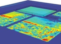
The shift from traditional 2D IC designs to 3D ICs brings a new set of thermal dynamics. In 2D designs, heat dissipation occurs primarily across a single plane, making it relatively straightforward to manage using conventional thermal management techniques. However, 3D ICs stack multiple active layers, each generating heat. This stacked configuration can lead to significant thermal gradients and hotspots, which can degrade device performance and reliability. Figure 2 illustrates die-level thermal analysis heat maps on a 2.5D layout.
Figure 2. Die-level thermal heat maps help designers find and repair hotspots in the 2.5D or 3D assembly.
In 3D ICs, the high power density and the proximity of multiple active layers exacerbate thermal issues. Heat generated in one layer can easily affect adjacent layers, leading to complex thermal interactions that are not present in 2D designs. The increased thermal coupling between dies and the package necessitates a thorough understanding and management of heat flow to prevent performance degradation and potential failure.
Early Floorplanning and thermal feasibility analysis
During initial floorplanning, designers can perform thermal feasibility studies using high-level power estimates and simplified models. This proactive approach reduces the likelihood of encountering critical thermal issues late in the design process, thereby shortening the overall design cycle.
For example, early thermal analysis can reveal issues such as overlapping heat sources in stacked dies or insufficient cooling paths. Figure 3 shows thermal hotspots overlaid on the design. Early analysis lets designers explore alternative floorplans and adjust power distribution to mitigate thermal risks.
Figure 3. Designers can inspect thermal effects by seeing hotspots overlaid on the design.
Iterative thermal analysis throughout design refinement
Thermal analysis should be performed iteratively as the design progresses and more detailed information becomes available to refine the thermal model and verify that the design remains within acceptable thermal limits. Each stage of design refinement has additional details such as power maps and layout geometries.
This iterative approach enables designers to continuously monitor and address thermal issues, ensuring that the design evolves in a thermally aware manner. By integrating thermal analysis with other design verification tasks, such as timing and power analysis, designers can achieve a holistic view of the design’s performance and reliability.
Tools and techniques for accurate thermal analysis
To effectively manage thermal challenges in 3D ICs, designers need advanced tools and techniques. Modern die-level thermal analysis tools are equipped with capabilities to handle the complexity of 3D IC designs and provide accurate and fast thermal analysis throughout the design flow.
High-fidelity thermal models
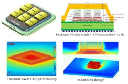
Accurate thermal analysis requires high-fidelity thermal models that capture the intricate details of the 3D IC assembly. These models should account for non-uniform material properties, fine-grained power distributions, and the thermal impact of through-silicon vias (TSVs) and other 3D features. Advanced tools can generate detailed thermal models based on the actual design geometries, providing a realistic representation of heat flow and temperature distribution (Figure 4).
Figure 4. Accurate boundary conditions and accurate chip models capture true thermal behavior of design.
For instance, tools like Calibre 3DThermal embed an optimized custom 3D Thermal solver from the Simcenter Flotherm tool to perform precise thermal analysis down to the nanometer scale. By leveraging detailed layer information and accurate boundary conditions, these tools can produce reliable thermal models that reflect the true thermal behavior of the design.
Automated thermal analysis and optimization
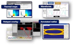
Automation is a key feature of modern thermal analysis tools, enabling designers to perform complex analyses without requiring deep expertise in thermal engineering. Automated gridding, power map compression, and equivalent thermal property extraction streamline the analysis process, allowing designers to focus on interpreting results and making design decisions. Results can be reviewed in thermal maps, waveforms, hotspot overlays, and an annotated SPICE netlist can be generated for electro-thermal simulation at the package level
Figure 5. Ways to view thermal analysis results.
Automated thermal analysis tools also integrate seamlessly with other design verification and implementation tools, providing a unified environment for managing thermal, electrical, and mechanical constraints. This integration ensures that thermal considerations are consistently addressed throughout the design flow, from initial floorplanning to final tape-out.
Case studies: the impact of early thermal analysis
Real-world examples demonstrate the effectiveness of early and continuous thermal analysis in improving 3D IC design outcomes. One such case is the INTACT design for massive parallel computing, developed by CEA. This design, composed of 16 chiplets on an active interposer, integrates a total of 96 cores. Early thermal-aware partitioning using coarse-grained power maps enabled the design team to explore different chiplet placements and optimize die-to-die interfaces (Figure 6).
Figure 6. INTACT 3D partitioning, lid and heatsink design.
By exporting the early thermal model to a system-level thermal analysis tool, the team optimized the thermal interface materials (TIM), copper lid, and heatsink design. The final signoff thermal analysis, which accounted for detailed 3D structures and fine-grained power maps, revealed important anisotropic thermal properties and heterogeneous hotspots. This comprehensive approach ensured that the design met its thermal budget and reliability requirements, while also reducing simulation time from days to less than an hour.
Conclusion: the path forward for 3D IC thermal management
As the industry continues to push the boundaries of integration and performance, the importance of accurate thermal analysis throughout the 3D IC design flow cannot be overstated. By incorporating thermal analysis early in the design process and iteratively refining thermal models, designers can mitigate thermal risks, reduce design time, and enhance chip reliability.
Advanced thermal analysis tools that integrate seamlessly with the broader design environment are essential for achieving these goals. These tools enable designers to perform high-fidelity thermal analysis, automate complex tasks, and ensure that thermal considerations are addressed consistently from floorplanning to signoff.
By embracing robust thermal analysis methodologies and tools, designers can unlock the full potential of 3D IC technology, delivering innovative, high-performance devices that meet the demands of today’s increasingly complex applications.


