This file type includes high resolution graphics and schematics when applicable.
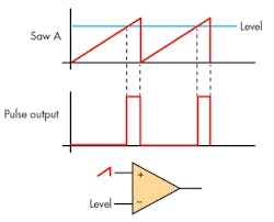
Pulse-width modulation (PWM) is used in applications ranging from controlling valves or pumps to adjusting the brightness of LEDs. In this proposed design, a PWM waveform is the basis for an analog-to-digital-converter (ADC) implementation. The PWM waveform can be easily generated through a comparator using a triangle or sawtooth waveform and variable dc voltage (Fig. 1). As the input varies from 0 to 10 VDC , the pulse width changes proportionately. A microcontroller reads the width digitally and displays the corresponding dc input voltage to the user after engineering conversion through the RS-232 port of a legacy machine.
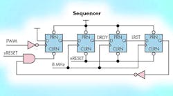
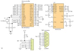
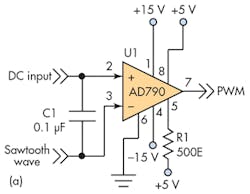
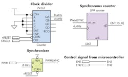
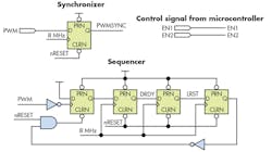
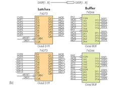
In this implementation of a proposed PWM converter approach, the two inputs to comparator U1 are the sawtooth waveform from an arbitrary waveform generator and the dc input from a precision voltage calibrator (Fig. 2a). The sawtooth has a negative offset to ensure that there’s a pulse when the dc input is zero; the sawtooth varies from –2 V to 10 V (12 VP-P). The digital circuit must measure the width of the generated output PWM pulse. This circuit is implemented in a CPLD, and consists of a synchronizer, counter, sequencer, latches, and three-state buffers (Fig. 2b), and interfaces to U2, a PIC microcontroller, and the RS-232 port (U3 and Conn1) (Fig. 2c).
The PWM pulse, which is synchronized with respect to the system clock, serves as an active-high count-enable signal of the 16-bit synchronous counter. The sequencer circuit generates two signals, DRDY and LRST, after the trailing edge of the PWM pulse to latch the synchronous counter output. Then it resets the counter to restart the fresh measurement and acquire new data. After synchronizing, it uses the pulse-width ON time to enable the counter, which is clocked by a fixed 4-MHz source (derived using the clock divider as shown).
The latched output is available through buffers, which are enabled by the microcontroller and subsequently read. EN1 and EN2 are the buffer-enable signals generated by the microcontroller to read the latched counter outputs for downstream processing. When the dc input varies from 0 to 9.95 V, the pulse width is measured with the counter. The sequencer, which is implemented with simple shift register, ensures that the counter output is reset only after latching into the register.
Since the count for 0 V dc is already known (both mathematically and empirically), the result for any value from 10 mV to 9.95 V is computed by subtracting the measured counts with the zero value. The equations for the width of the PWM waveform and factors are:
• TW = TP × (|VNeg-pk | + VDC)/ VP-P,
• Synchronous counter output value = TW × TCLK
• Float Normval = (counter output – count offset) × scaling factor
• Int ADCVAL = Normval – Lin factor
where:
TW = pulse width (ms)
TP = time period of sawtooth wave
• V|Neg-pk | is the peak negative voltage, taken in absolute scale
• VDC = 0-10 V dc input voltage
• VP-P = peak-to-peak voltage levels of sawtooth waveform
• TCLK = the sampling clock to the synchronous counter
• Count offset = the counts corresponding to VDC = 0 V
• Normval = a software variable multiplied by appropriate scaling factor
• ADCVAL = a software variable indicating the final ADC count value (in millivolts) after the linear factor correction (Lin factor).
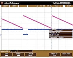
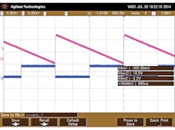
For the proposed design, VP-P = 12 V, |VNeg-pk | = 2 V, and TP = 2 ms (500-Hz period) were chosen. This resulted in a pulse width ranging from 333 µs for VDC = 0 V to approximately 2 ms for VDC = 9.95 V. The corresponding counter outputs varied from 1332 (min) to 8000 (max) count, respectively, for TCLK = 4 MHz.
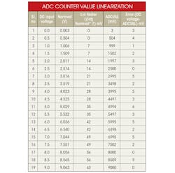
The scaling factor is evaluated by the formula (8000 -1332) × scaling factor = 10 V. Here, the scaling factor worked out to be 1.5 (mV). Linear factor is evaluated after tabulating the measured value of ADCVAL for the corresponding input dc voltage and estimating the slope by curve fitting (see the table). The Lin factor was derived as ((Int)Normval × 7) mV.
The scope photos (Figs. 3 and 4) show the output pulse widths for dc inputs of 8 and 4 V, respectively. The output results for this PWM-based approach to implementing an ADC shows only minor variations compared to the expected value. The tabulated value indicates that the proposed design functions as a 10-bit ADC.
G.V.Kishore and K.Palanisami are with the Power Electronics Section, Electronics & Instrumentation Division, Indira Gandhi Centre for Atomic Research (IGCAR), Kalpakkam-603102, Tamilnadu, India.
This file type includes high resolution graphics and schematics when applicable.
