JESD204B vs. Serial LVDS: Interface Considerations for Wideband Data-Converter Apps
The JESD204A/JESD204B industry standard for serial interfaces was developed to address the problem of interconnecting the newest wideband data converters with other system ICs in an efficient and cost-saving manner. The motivation was to standardize an interface that would reduce the number of digital inputs/outputs between data converters and other devices, such as field-programmable gate arrays (FGPAs) and system-on-chip (SoC) devices through the use of a scalable high-speed serial interface.
Trends show that new applications, as well as advances in existing ones, are driving the need for wideband data converters with increasingly higher sampling frequencies and data resolutions. Transmitting data to and from these wideband converters poses a significant design problem, as bandwidth limitations of existing I/O technologies force the need for higher pin counts on converter products.
Consequently, systems’ PCB designs have become increasingly more complex in terms of interconnect density. The challenge is routing a large number of high-speed digital signals while managing electrical noise. The ability to offer wideband data converters with GS/s sampling frequencies, using fewer interconnects, simplifies the PCB layout challenges, and it allows for smaller form-factor realization without impacting overall system performance.
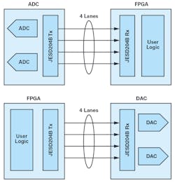
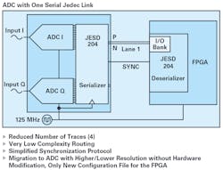
Market forces continue to press for more features, functionality, and performance in a given system, driving the need for higher data-handling capacity. The high-speed analog-to-digital converter and digital-to-analog converter-to-FPGA interface had become a limiting factor in the ability of some system OEMs to meet their next-generation data-intensive demands. The JESD204B serial interface specification was specifically created to help solve this problem by addressing this critical data link. Figure 1 shows typical high-speed converter-to-FPGA interconnect configurations using JESD204A/JESD204B.
Some key end-system applications that are driving the deployment of this specification, as well as a contrast between serial low-voltage differential signaling (LVDS) and JESD204B, are the subject of the remainder of the article.
The Applications Driving the Need for JESD204B
Wireless Infrastructure Transceivers
Technologies based on orthogonal frequency-division multiplexing (OFDM), such as LTE, used in today’s wireless infrastructure transceivers use DSP blocks implemented on FPGAs or SoC devices driving antenna-array elements to generate beams for each individual subscriber’s handset. Each array element can require movement of hundreds of megabytes of data per second between FPGAs and data converters in both transmit or receive modes.
Software-Defined Radios
Today’s software-defined radios (SDRs) utilize advanced modulation schemes that can be reconfigured on-the-fly, as well as rapidly increasing channel bandwidths, to deliver unprecedented wireless data rates. Efficient, low-power, low-pin-count FPGA-to-data converter interfaces in the antenna path play a critical role in their performance. SDR architectures are integral to the transceiver infrastructure for multicarrier, multimode wireless networks supporting GSM, EDGE, W-CDMA, LTE, CDMA2000, WiMAX, and TD-SCDMA.
Medical Imaging Systems
Medical imaging systems including ultrasound, computational tomography (CT) scanners, and magnetic-resonance imaging (MRI), and others generate many channels of data that flow through a data converter to FPGAs or DSPs. Continually increasing I/O counts are driving up the number of components by requiring the use of interposers to match FPGA and converter pin out and increasing PCB complexity. This adds more cost and complexity to the customer’s system, which can be solved by the more efficient JESD204B interface.
Radar and Secure Communications
Increasingly sophisticated pulse structures on today’s advanced radar receivers are pushing signal bandwidths toward 1 GHz and higher. The latest-generation active electronically scaled array (AESA) radar systems may have thousands of elements. High-bandwidth SERDES-based serial interfaces are needed to connect the array-element data converters to the FPGAs or DSPs that process incoming, and generate outgoing, data streams.
Choosing Between Serial LVDS and JESD204B Interface
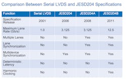
To best select between converter products that use either LVDS or the various versions of the JESD204 serial interface specification, a comparison of the features and capabilities of each interface is useful (see table).
At the SERDES level, a notable difference between LVDS and JESD204 is the lane data rate, with JESD204 supporting greater than three times the serial-link speed per lane when compared with LVDS. When comparing the high-level features like multidevice synchronization, deterministic latency, and harmonic clocking, JESD204B is the only interface that provides this functionality. Systems requiring wide-bandwidth multichannel converters that are sensitive to deterministic latency across all lanes and channels won’t be able to effectively use LVDS or parallel CMOS.
LVDS Overview
LVDS is the traditional method of interfacing data converters with FPGAs or DSPs. LVDS was introduced in 1994 with the goal of providing higher bandwidth and lower power dissipation than the existing RS-422 and RS-485 differential transmission standards. LVDS was standardized with the publication of TIA/EIA-644 in 1995. The use of LVDS increased in the late 1990s and the standard was revised with the publication of TIA/EIA-644-A in 2001.
LVDS uses differential signals with low-voltage swings for high-speed data transmission. The transmitter typically drives ±3.5 mA with a polarity matching the logic level to be sent through a 100-Ω resistor, generating a ±350-mV voltage swing at the receiver. The always-on current is routed in different directions to generate logic ones and zeros.
The always-on nature of LVDS helps eliminate simultaneous switching noise spikes and potential electromagnetic interference that sometimes occur when transistors are turned on and off in single-ended technologies. The differential nature of LVDS also provides considerable immunity to common-mode noise sources. The TIA/EIA-644-A standard recommends a maximum data rate of 655 Mb/s, although it predicts a possible speed of over 1.9 Gb/s for an ideal transmission medium.
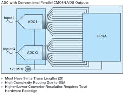
The huge increase in the number and speed of data channels between FPGAs or DSPs and data converters, particularly in the applications described earlier, has created several issues with the LVDS interface (Fig. 2). The bandwidth of a differential LVDS wire is limited to about 1.0 Gb/s in the real world. In many current applications, this creates the need for a substantial number of high-bandwidth PCB interconnects, each of which is a potential failure point. The large number of traces also increases PCB complexity or overall form factor, which raises both design and manufacturing costs. In some applications, the data-converter interface becomes the limiting factor in achieving the required system performance for bandwidth-hungry applications.
JESD204B Overview
The JESD204 data-converter serial interface standard was created by the JEDEC Solid State Technology Association JC-16 Committee on Interface Technology. The goal was to provide a higher-speed serial interface for data converters to increase bandwidth and reduce the number of digital inputs and outputs between high-speed data converters and other devices. The standard builds on 8b/10b encoding technology developed by IBM that eliminates the need for a frame clock and data clock, enabling single-line-pair communications at a much higher speed.
In 2006, JEDEC published the JESD204 specification for a single 3.125-Gb/s data lane. The JESD204 interface is self-synchronous, so there’s no need to calibrate the length of the PCB wire traces to avoid clock skew. JESD204 leverages the SERDES ports offered on many FPGAs to free up general-purpose I/O.
JESD204A, published in 2008, adds support for multiple time-aligned data lanes and lane synchronization. This enhancement makes it possible to use higher-bandwidth data converters and multiple synchronized data-converter channels. It’s particularly important for wireless infrastructure transceivers used in cellular base stations. JESD204A also provides multidevice synchronization support that’s useful for devices, such as medical imaging systems, that utilize large numbers of ADCs.
JESD204B, the third revision of the spec, increases the maximum lane rate to 12.5 Gb/s. JESD204B adds deterministic latency, too, which communicates synchronization status between the receiver and transmitter. Harmonic clocking, also introduced in JESD204B, makes it possible to derive a high-speed data-converter clock from a lower-speed input clock with deterministic phasing.
Conclusion
The JESD204B industry serial interface standard reduces the number of digital inputs and outputs between high-speed data converters and FPGAs and other devices. Fewer interconnects simplify layout and make it possible to achieve a smaller form factor (Fig. 3). These advantages are important for a wide range of high-speed data-converter applications, such as wireless infrastructure transceivers, software-defined radios, medical imaging systems, and radar and secure communications.
Analog Devices is an original participating member of the JESD204 standards committee, and the company has concurrently developed compliant data-converter technology and tools along with a product roadmap. By providing customers with products that combine its data-converter technology along with the JESD204A/JESD204B interface, it should help solve system design problems while leveraging this interfacing breakthrough.
George Diniz is a Product Line Manager in the High Speed Digital-to-Analog Converters Group at Analog Devices.
