Download this article in PDF format.
There’s increasing demand for ultra-high precision measurements that can achieve greater than 24-bit resolution in industries from aerospace and defense and gas exploration to pharmaceutical and medical-device manufacturers. For example, the pharmaceutical industry uses high-precision lab balances that offer 0.0001-mg resolution over a 2.1-g full-scale range that would require an analog-to-digital converter (ADC) with greater than 24-bit resolution. Calibration and testing of these high-precision systems challenges the instrumentation industry to offer test equipment that can achieve greater than 25-bit resolution with at least 7.5-digit measurement precision.
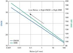
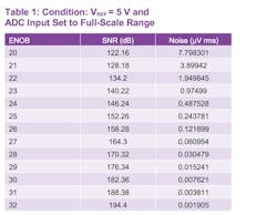
To achieve this high resolution, a signal chain with exceptionally low noise is required. Figure 1 shows the relationship of noise versus effective number of bits (ENOB) and signal-to-noise ratio (SNR). Note noise is calculated based on voltage reference (VREF) equal to 5 V and ADC input set to full-scale range. To provide perspective, to achieve 25-bit resolution, or 152-dB dynamic range, the maximum allowable system noise is 0.2437 µV rms.
The voltage reference sets the limit to the input analog signal that the ADC can resolve. Equation 1 is the ideal transfer function of an ADC where the output code—in decimal form—is computed by the analog input signal VIN, voltage reference VREF, and number of ADC bits N.
Typically, the resolution stated in the ADC datasheet is based on an input-shorted technique where the ADC input is connected to the GND or the ADC differential inputs are connected to a common source. The ADC input-shorted technique helps to characterize the absolute limit of the ADC resolution by omitting the ADC input source noise and eliminating the effect of VREF noise. This is true because VIN is set to 0 V, resulting in the ratio VIN/VREF being equal to 0 V.
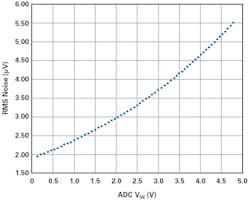
To investigate the effects of the voltage-reference noise’s overall system noise, Figure 2 shows the relationship between total system noise (rms) with ADC input dc source voltage. For this test, we used the AD7177-2 32-bit ADC with the VREF input connected to the LTC6655-5 (5 V) and the ADC input connected to a low-noise dc source. The ADC output data rate was set to 10 kS/s. Note, throughout the ADC input voltage range, the ADC noise remains constant (35 nV/√Hz), while the ADC dc input source noise rises (≤6 nV/√Hz) but remains low in comparison to the voltage-reference noise (96 nV/√Hz).
As shown in Figure 2, the total noise is proportional to the ADC dc input voltage. This is because as VIN increases, the ratio VIN/VREF increases. Thus, the VREF noise dominates the overall system noise when the ADC is at full-scale input. The individual noise of each component in the signal chain adds together in root-sum-square (RSS) fashion and gives rise to the shape of the curve in Figure 2.
To achieve a high measurement resolution of 25 bits or beyond, even the best standalone voltage references available in the market with a low-noise specification needs some help to attenuate its noise. Adding external circuitry such as a filter can help attenuate noise to achieve the desired ADC dynamic range.
The remainder of this article explains various types of low-pass filters (LPFs) and how this can be applied to attenuate voltage-reference noise. Filter design techniques and filter tradeoffs are discussed. Also examined are two types of LPFs in the context of attenuated voltage-reference noise: simple passive RC LPFs and active-based signal-flow-graph (SFG) LPFs. System evaluation results using a sigma-delta (∑-Δ) ADC will be presented in the circuit performance section.
Noise Reduction Using a Passive Low-Pass Filter
Figure 3 shows the voltage reference driving an ADC via an LPF implemented with an external reservoir capacitor (C1), the equivalent series resistance (ESR) of the reservoir capacitor, and the output impedance of the voltage-reference operational amplifier (op amp). The passive RC LPF cutoff frequency is determined by:
which states that bandwidth is inversely proportional to resistance R and capacitance C.
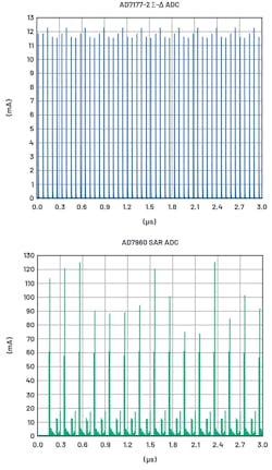
Reservoir capacitor C1 also works as local energy storage to compensate for voltage spikes caused when ADC voltage-reference circuitry demands sudden change in load current. Figure 4 shows the sigma-delta AD7177-2 and SAR AD7980 ADC dynamic reference current response.
The user can choose the value of the C1 capacitor to meet the LPF cutoff frequency requirement, but some SAR ADCs require a 10-µF-minimum capacitor on the reference input to operate correctly. This 10-µF C1 capacitor reduces the phase margin of the reference buffer. As the phase margin reduces, the buffer feedback is no longer negative.1 The signals near the unity-gain crossover frequency are fed back in-phase with the incoming signals.1 This causes the closed-loop response to introduce noise peak near the crossover frequency.1 Since the bandwidth from the cutoff frequency (–3 dB point) reaches up to 16 MHz, the total integrated noise (rms) is dominated by the noise peak.
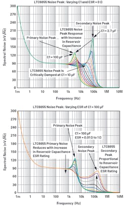
Even though voltage-reference reservoir capacitor C1 operates as a noise filter and compensates for voltage spikes, the caveat is the noise peak. Figure 5 shows the noise peak of the LTC6655 voltage reference introduced by reservoir capacitor C1. The noise peak magnitude is determined by the value of the reservoir capacitor and its ESR rating.
Most voltage references are designed with a complex output stage to drive a large load capacitance suitable for ADC reference circuitry. For example, the LTC6655 output stage is designed to be critically damped with a reservoir capacitance set to 10 µF. When the LTC6655’s reservoir capacitance is set to a minimum of 2.7 µF and a maximum of 100 µF, noise peaking is introduced.
Though the equivalent series resistance (ESR) of the VREF output reservoir capacitance does mitigate the primary noise peak, it introduces a secondary noise peak at 100 kHz and above. This can be explained by the fact that the ESR of the cap introduces a zero, which leads to improving phase margin and reducing primary noise peak. However, this zero combines with the inherent zero of the LTC6655 and creates secondary noise peaking. Note, the noise response in Figure 5 is only valid for the LTC6655 voltage reference.
One of the other solutions to filter voltage-reference noise, remove the noise peak, and properly drive the ADC is to add a passive RC LPF followed by a buffer. By adding a buffer, we separate the design constraints of the LPF and the ADC reference input capacitor (Fig. 6).
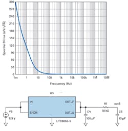
Setting the passive RC LPF cutoff frequency well below the unity-gain crossover frequency will not only reduce broadband and low-frequency noise, but also avoid noise peaking. For example, Figure 7 shows the LTC6655 noise response with C1 = 100 µF (ESR = 0 Ω), followed by a passive LPF where R = 10 kΩ and C2 = 10 µF (ESR = 0 Ω), creating a pole at 1.59 Hz.
Increasing the low-pass filter resistor R can help achieve a low cutoff frequency, but it can also result in dc accuracy degradation of a precision voltage reference. When adding a passive RC LPF, the user must also consider the impact on the load regulation and the impact on the VREF buffer response (τ = RC), which affects its transient performance when driving an ADC.
To achieve the required transient performance, it’s suggested to use a buffer as shown in Figure 6. Critical specifications to consider in terms of selecting a buffer includes ultra-low noise, capability to support high load capacitance, low distortion, excellent slew rate, and wide gain bandwidth. Examples of reference buffers are the ADA4805-1 and ADA4807-1.
Noise Reduction Using an Active LPF
Table 1 states the required dynamic range and maximum allowable system noise that must be met to achieve the desired ENOB ADC resolution. Depending on the ADC bandwidth, a single-pole LPF attenuating at 20 dB/decade may not achieve the desired wideband noise reduction. Cascading passive LPFs creates a ladder structure that can generate a higher-order filter, but each section’s input impedance will be a load on the previous section. This can degrade the dc accuracy of the precision voltage reference.
However, designing a higher-order LPF based on active components will provide excellent isolation between input to output, minimizing voltage reference dc accuracy degradation, and provide low output impedance to drive the reference circuitry of the ADC.
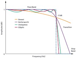
There are several different types of active low-pass filters—for example, Bessel, Butterworth, Chebyshev, and elliptic (Fig. 8). Having a bandpass that’s flat or doesn’t exhibit ripple will keep the precision voltage reference’s dc accuracy degradation to a minimum. Out of all filter types, designing an LPF based on the Butterworth topology can achieve flat bandpass and steep attenuation.
Active Low-Pass Filter Design Technique
A signal flow graph is a graphical representation of a system derived from a set of linear equations.2 An SFG provides a bridge from a transfer function to a corresponding circuit topology of a system.2 This theory can be applied to designing analog filters based on active circuitry.
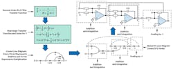
The key advantage of an SFG filter design approach is that the damping factor, Q, and cutoff frequency can be individually controlled. An SFG LPF can help attenuate noise and improve SNR, but it comes at the cost of additional bill of materials (BOM) expenses, PCB area, and power. Furthermore, an SFG LPF can affect the reference output voltage with temperature, leading to a small PPM error and hence dc accuracy degradation. Figure 9 shows an example of second-order LPF transitioning from transfer function to circuit blocks via the SFG method. The scaling resistor (R) and capacitor (C) configures for the cutoff frequency (see Equation 5).
where Rs is scaling factor, Cn is scaling factor, and Ws is cutoff frequency (Rad/s).
For more details about SFG theory, please refer to Feedback Control of Dynamic Systems, published by Addison-Wesley.2
The following is a calculation example for designing a second-order, 0.5-Hz cutoff frequency SFG low-pass Butterworth filter:
- One 10-kΩ resistor
- One 39-pF capacitor
- One 1N4001 diode
- For simplicity of this example, select Rs = 1 Ω, Cn = 1 F.
- Select Fs = 0.5 Hz to maximize rejection of broadband noise; Ws = 2 × π × 0.5 = 3.141 rad.
- Set the damping factor Q = 0.71. Select this value to achieve a flat bandpass and steep attenuation to reflect Butterworth topology.
- R, C, and Rq values were chosen based on an iterative process to achieve low thermal noise and the availability of component values for surface-mount.
Low-Pass Filter
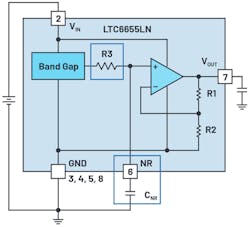
Considering the RC LPF and SFG LPF tradeoffs, a better solution is to have an LPF placed before the integrated low-noise buffer of the voltage reference (Fig. 10). This implementation will not only reduce the PCB area, but also not hinder the voltage-reference buffer response. Using a voltage-reference buffer with fast settling, high input impedance, and the capability to sink and source current will help overcome poor load regulation, maintain dc accuracy, and improve transient performance.
The LTC6655LN, for example, is built around this architecture. It comes with a noise-reduction pin that enables reduction of wideband noise and an integrated output-stage buffer. Internally equipped with an R3 resistor (Figure 10, again), this allows users to connect an external capacitor at the noise-reduction (NR) pin to create an LPF (Table 2). With such an architecture, users can configure the low-pass cutoff frequency based on their system requirements. It also eliminates the need for an external buffer to drive ADC voltage-reference circuitry.
The RC LPF is connected to the noninverting node of the buffer, which is the most sensitive pin on this device. Precaution must be taken when selecting a low-leakage type for the external capacitor to prevent leakage current flow through the R3 resistor, which can degrade dc accuracy (Table 3). Furthermore, the variation of R and C don’t track each other; therefore, the RC time constant and LPF cutoff frequency can change due to process, voltage, and temperature (PVT) variation.
Test Circuit Description
The AD7177-2 precision ADC was used to benchmark the performance of LTC6655/LTC6655LN with a 10-µF NR capacitor and LTC6655 followed by an active SFG filter. The AD7177-2 is a high-resolution, 32-bit, low-noise, fast-settling, 2-channel/ 4-channel, sigma-delta ADC for low bandwidth inputs. It’s integrated with a programmable digital LPF that allows users to control the output data rate (ODR) from 5 samples per second to 10 kS/s.
The components used in designing the SFG LPF (Fig. 11) were two ADA4522-1 op amps, an AD797 op amp, 25-ppm surface-mount resistors, multilayer surface-mount ceramic capacitors, and a 10-µF WIMA film capacitor. The ADA4522 is a rail-to-rail output op amp with a broadband noise density of 5.8 nV/√Hz and 177 nV p-p flicker noise. The AD797 is a low-noise op amp with 0.9 nV/√Hz broadband noise, 50 nV p-p flicker noise, slew rate of 20 V/µs, and gain bandwidth of 100 MHz, which makes it suitable for driving an ADC.
To correctly evaluate the performance when using a LTC6655 and a LTC6655LN with an AD7177-2, a dc source with overall noise lower than the ADC voltage reference and the ADC noise is required. Therefore, an ideal source was used, namely a 9-V battery supply (Fig. 12).
Circuit Performance
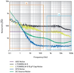
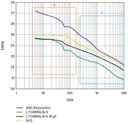
Figure 13 displays spectral noise density and Figure 14 reveals output data rate (ODR) vs. ENOB, depicting the performance of AD7177-2 with its VREF input connected to a LTC6655/LTC6655LN with a 10-µF NR capacitor or filtered LTC6655 (SFG). Table 4 provides perspective of the spectral noise density comparison at 1 kHz.
Both Figures 13 and 14 have two important regions:
Region A
The spectral noise density plot in Figure 13 shows that at ODR of 500 samples/s and higher, both the filtered LTC6655 (SFG) and ADC dc input source noise are significantly lower noise than the ADC. This results in the least amount of deviation from the maximum performance achievable by the ADC as shown in region A in Figure 14. The key takeaway based on ODR vs. ENOB and the spectral noise density plot is that, within region A, the rise of the total integrated noise (rms) prevents the signal chain from achieving 25-bit measurement resolution.
Region B
In this region, the spectral noise density plot (Fig. 13) shows that the flicker noise of the three voltage-reference options and the dc source increase and overall system noise are dominated by the dc source noise. This increase in flicker noise within region B explains the rise in deviation of ENOB between the measured performance and maximum achievable by the ADC (Fig. 14).
According to the ODR vs. ENOB plot, filtered LTC6655 (SFG) achieves 25-bit resolution at 20 samples/s and lower, while the LTC6655LN-5 with 10-µF NR capacitance and the LTC6655 can’t achieve better than 24.6-bit resolution.
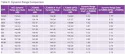
Table 5 is a summary of the AD7177-2 ADC performance with the VREF input either connected to a LTC6655/LTC6655LN with 10-µF NR capacitance or filtered LTC6655 (SFG). With ADC inputs tied together and the VREF input connected to LTC6655, the zero-scale column establishes the best dynamic range achievable with the AD7177-2.
With the ADC inputs nearly set to full-scale range, the LTC6655LN-5 with 10-µF NR capacitance increases on average 4-dB dynamic range for up to 59.96 samples/s/ compared to LTC6655. On the other hand, a filtered LTC6655 (SFG) achieves on average a 7-dB increment in dynamic range compared to LTC6655 for up to 59.96 samples/s. The dynamic range delta doesn’t vary much below 59.96 samples/s and the variance is mainly due to the dominated low-frequency flicker noise induced by the ADC input dc source.
LTC6655/LTC6655LN with 10 µF connected to the NR pin reduces the broadband noise at 1 kHz by 62%, and the filtered LTC6655 (SFG) reduces broadband noise by 97%.
Conclusion
A precision system that’s attempting to achieve a 25-bit resolution or higher must account for the significance of voltage-reference noise. As shown in Figure 2, the contribution of VREF noise to system noise is proportional to the utilization of the ADC’s full-scale range. This article shows that adding a filter to a precision voltage reference attenuates VREF noise, which leads to reduced overall system noise.
A voltage reference followed by an SFG filter can reduce broadband noise by 97% of the voltage reference with no filter. This comes at a cost of additional BOM, more PCB area, more power consumption, and a few PPM of dc accuracy degradation, and can vary precision reference output with temperature. Considering SFG LPF tradeoffs, an integrated approach provides a more simple design, low power, only requires a single capacitor to reduce broadband noise, and eliminates the need for an external buffer to drive an ADC.
Acknowledgements
I would like to thank author Robert Kiely for his previous work on sigma-delta ADCs, precision amplifiers, and voltage references.
Anshul Shah is an Applications Engineer in the Instrumentation and Precision Technology Group at Analog Devices.
References
1. Mark Reisiger. “Reduce Amplifier Noise Peaking to Improve SNR.” Electronic Design, October 2012.
2. Gene F. Franklin, J. David Powell, and Abbas Emami-Naeini. Feedback Control of Dynamics Systems. Addison-Wesley Longman Publishing Co., Inc., November 1993.

