11 Myths About Signal Integrity in High-Density Backplanes
As a signal travels across a network, it focuses only on what it sees in its path. And increases in data rates over the past few decades have made this path a bit more clouded. System infrastructure needs to accommodate such increases through better bandwidth management, better system interoperability, and higher data throughput. This is no short order.
Many of these challenges are being handled in the backplane, which manages much of the interconnect between various circuit boards or cards across a system. By cramming more electrical connections into the same footprint, high-density backplanes seem to invite signal-integrity (SI) issues, making some embedded designers skeptical about how to best move this influx of data within their applications. Here, we explore what can be accomplished using a high-density backplane, while preserving signal integrity across the network.
1. Signal-integrity analysis considerations are different in nature, depending on the backplane architecture/topology/technology.
Signal integrity typically looks at the same parameters of the backplane channels—insertion loss, return loss, operating margin, crosstalk, etc.—irrespective of the building blocks of the channel, how the system is architected, or the intended data rates. The acceptable limits of these parameters are what vary, depending on the protocol/data rate.
Although SI is not a function of form factor, considerations do exist that may be somewhat affected by topology. Solutions to optimize signal integrity require versatility in their approach in order to properly measure different backplane parameters (topology, lengths, geometry), especially with increasing system density.
2. Data provided by the connector and PCB manufacturers have no bearing on the results of pre- and post-layout signal-integrity analysis of channels.
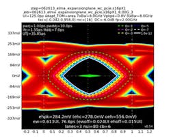
It’s essential that the data provided by both connector manufacturers and PCB manufacturers first be vetted for, and then incorporated into, the analysis performed. For instance, this data is critical to the optimization and analysis of the PCB stackup, trace geometry parameters, as well as physical and electrical models for the connectors (Fig. 1).
3. Links in a backplane-based system are independent of one another, and therefore don’t affect overall performance.
Each link in these types of systems will contribute to system performance and potentially affect the performance of otherwise good links, causing bottlenecks in bandwidth across the entire system via excessive crosstalk. Provisions to simulate and measure all problematic (worst case) links within a design need to be incorporated into a system-level signal-integrity analysis.
4. The behavior of a complete channel is the sum of the behaviors of its individual sub-sections.
At higher data rates, the behavior of a complete channel isn’t always accurately represented by just a concatenation of individually simulated/measured blocks. Or in the words of Aristotle, “The totality is not, as it were, a mere heap, but the whole is something besides the parts.” Cascading the models of individual blocks is warranted, only if the points at which the cascading is done are those with very low reflections, which in most cases (like connector interfaces) is patently false.
That’s why co-design, or cooperation at the layout stage, is an important aspect of an embedded system. Developing a system in parallel can reduce signal-integrity issues, yielding better return loss and, more importantly, much better insertion loss.
5. The type of weave used on the layers that carry high-speed signals has no bearing on signal integrity and, therefore, isn’t a critical consideration.
The weave does impact signal integrity as the data rate increases. With the advent of protocols that require lower intra- and inter-pair skew, fiber-weave-induced skew may make or break the performance of some of the longer links in a system. Careful consideration must be given to the compromise between a spread weave choice and the resin content for a given laminate material.
The long-held assumption that the dielectric material surrounding the traces in the backplane or daughtercard PCBs is almost homogenous and isotropic in all directions is not only demonstrably false, but dangerous to make for high-data-rate transmission channels.
6. You can expect simulations to be close to measurements, even without validating your models.
Simulation at the pre- and post-layout stage is a necessary step. However, without using validated models, your simulations will only be as good as the assumptions built into those models. Vetting S-parameter models for passivity and causality, and verifying the validity of a particular laminate material’s properties, are just two examples.
7. The values of copper foil roughness and resistivity given by PCB laminate manufacturers, and even those in empirical formulas, are pretty close to reality.
Apart from the values given in manufacturers’ datasheets, typical models used in SI simulations for copper surface roughness include the Huray snowball model and Hammerstad. However, these datasheet values and theoretical models must be correlated with actual measurements of the copper foil as processed by the PCB manufacturer. Different PCB fab houses employ different methods and equipment for roughening the copper foil’s surface for better adherence to the substrate. How well the theoretical models used in simulations reflect reality is something worth investigating, because it affects the simulation’s accuracy (see Myth 6).
8. Developing design rules to test signal integrity should be conducted up to the limit of the application.
To truly test for signal integrity, it’s important to go beyond the scope of the application and account for worst-case scenarios to ensure your system, and your signals, will hold up under all circumstances. This “margin” allows for spikes in data transfer, higher than normal system loads, and less optimal designs of other components in the system (plug-in modules, mezzanine cards, power supplies, etc.).
9. The mated interface to the backplane isn’t important when considering the performance of a backplane PCB.
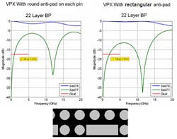
To properly model the signal path, the mated connector interface absolutely must be considered. The signal budget is affected by the plug-in cards that mate to the backplane, the backplane itself, and the connectors used as interfaces between the plug-in cards and backplane. Moreover, it’s not only the electromechanical properties of these mated connector interfaces that affect the signal budget, it’s also the footprint used for these connectors both on the plug-in cards and on the backplane (things like pad and anti-pad size, trace routing geometry in the area where it connects to the footprints, etc.) (Fig. 2).
10. Any simulation software and any de-embedding approach would do a decent job at analyzing SI data and making accurate predictions (i.e., “all SI tools are created equal and it only depends on the user’s ability of how accurately they make predictions about interconnect performance”).
While one would be tempted to consider simpler and oftentimes cheaper solutions for SI, one must be aware that—as is the case with everything else in life—you get what you pay for. “Half-baked” solutions may get it right sometimes (even a broken clock is right twice a day), but investing diligently in proven simulation tools, test equipment, calibration, and de-embedding techniques goes a long way to achieving good correlation between simulations and measurements, which is key to a successful approach to SI.
11. At the end of the day, if my backplane meets the signal budget allocated to it, even within the slightest margin, everything will run smoothly.
As was mentioned in previous myths, one must approach even individual sub-component design with a holistic methodology. A poor (or marginally good) launch from a plug-in module into a backplane will only get worse. With the backplane being a passive element of an end-to-end channel, it can’t improve the signal quality because it will add loss (different kinds of loss, too). Similarly, a backplane design with poor margins may actually result in a system failing.
Ovidiu Mesesan is Senior Engineer at Elma Electronic.


