Unique SiGe Growth Yields a Major Step to Using Silicon as a Photon Source
Since the start of the germanium- and silicon-based solid-state device era along with the availability of light-emitting diodes (LEDs), researchers have searched for a way to combine the capabilities of the two functions and their constituent materials. The result would be a match “made in heaven” as, at least in principle, the same die and processes used for the electronic circuitry could also provide the optical source for intrachip and interchip links. Thus, it would overcome the many costs associated with separate electro-optical modules.
However, despite decades of work pursuing the goal of achieving efficient light emission from group-IV materials in silicon technology, progress has been slow and often frustrating. The underlying problem is that cubic (crystalline) silicon (Si), germanium (Ge), and SiGe alloys are all indirect-bandgap semiconductors that can’t emit light efficiently.
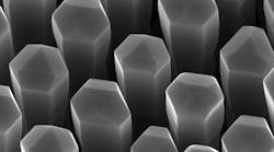
Leaping that hurdle, a team of researchers from the Technical University of Eindhoven (TU/e; Netherlands) and the Technical University of Munich (TUM; Germany) has developed light-emitting SiGe alloys, increasing the feasibility of development of a silicon-based laser that could be directly integrated into chips. Their success in demonstrating efficient light emission from direct-bandgap hexagonal Ge and SiGe alloys is the outcome of an effort that started in 2015, when Prof. Erik Bakkers and his team at TU Eindhoven first produced a hexagonal silicon structure with nanowires made of another material (Fig. 1).
1. Overview of the hex-Si1-xGex material system: (a) Schematic illustration of the hexagonal GaAs/Ge ore/shell nanowires drawn in blue/red, respectively. (b) Tilted-view scanning electron micrograph of an array of epitaxial GaAs/Ge nanowires grown on a GaAs (111)B substrate in the [0001] crystallographic direction. (c) Overlapped images of a cross-sectional thin layer (lamella) of a representative GaAs/Ge core/shell nanowire. (d) Aberration-corrected image of the interface of GaAs/Ge structure obtained in the [1120] zone axis, displaying the stacking along [0001] of the hexagonal crystal structure.
This served as a template for a germanium-silicon shell on which the underlying material imposed its hexagonal crystal structure (Fig. 2).
2. Growth process: (a) The core nanowire growth starts with a GaAs (111)B substrate patterned with Au catalyst seeds, which is introduced in the MOVPE reactor and annealed at a temperature higher than the eutectic temperature, forming an alloy between the catalyst seed and the substrate. (b) Next, the GaAs gas are introduced, and Au-catalyzed GaAs core nanowires are grown. To proceed with the SiGe shell growth, Au seeds are chemically etched away from the GaAs cores and the surface of the cores is repaired. (c) Then the sample is reintroduced to the MOVPE reactor. (d) A hex-Si1 − xGex shell is epitaxially grown around the GaAs cores from precursors (Si2H6 and GeH4).
“This material has a direct bandgap, and can therefore emit light itself,” says Prof. Jonathan Finley, Professor of Semiconductor Quantum Nanosystems at TUM. Initially, however, these structures could not be stimulated to emit light. To advance the effort, colleagues at TUM analyzed the optical characteristics with each successive generation of the grown structure, ultimately yielding a production process optimized to a grade of perfection where the nanowires were indeed capable of emitting light.
The team was able to measure a sub-nanosecond, temperature-insensitive radiative recombination lifetime and then observe an emission yield similar to that of direct-bandgap group-III–V semiconductors such as InGaAs/InP (Fig. 3). As a further enhancement, they were able to tune emission wavelength continuously over a broad range while preserving the direct bandgap by controlling the composition of the hexagonal SiGe alloy.
3. External radiative efficiency: (a) Integrated photoluminescence intensities of hex-SiGe in comparison with high-quality InGaAs/InP multiple quantum well (MQW) samples as measured in a micro- photoluminescence setup using 1030-nm wavelength, 125-pJ pulses. (b) Cross-sectional schematic diagramming the layer structure of the InGaAs/InP MQW sample, showing a total absorption thickness of 625 nm. (c) Schematic illustration of the geometry of the horizontally oriented hex-SiGe nanowire, showing the emission into a numerical aperture (NA) = 0.48 Cassegrain objective with a NA = 0.22 obscurity; the polarization of the emitted light is shown as V (vertical) and H (horizontal).
The results of the work are bolstered by the fact that this isn’t just a case of mixing and trying until the “magic” combination was found. Instead, they developed the underlying optical and quantum theory from first principles to support their direction and results, reporting that their experimental findings are in close quantitative agreement with the substantiating theory. They concluded that hexagonal SiGe is an ideal material system to use for combining electronic and optoelectronic functionalities on a single chip, opening the way toward integrated device concepts and information-processing technologies.
Results are in their lengthy and detailed Nature paper “Direct-bandgap emission from hexagonal Ge and SiGe alloys,” which is behind a paywall (although its “Extended data figures and tables” section is not blocked)—however, the entire technical package is also posted and available here.


