Combining Capacitors and Inductors in a Single Component
This article appeared in Machine Design and has been published here with permission.
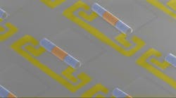
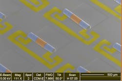
Researchers at the University of Illinois, Urbana-Champaign have devised a method of combining capacitors and inductors in a tiny, 3D rolled membrane. This will save space in the electronic filters found in phones and other wireless devices. They eliminate or enhance specific input signals to get the best output signals. While essential, these filters take up space on the chips that researchers are constantly trying to make smaller.
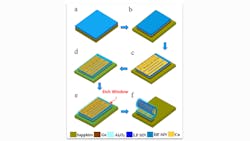
In the lab, the team used a specialized etching and lithography process to pattern 2D circuits onto thin membranes. In the circuits, they join capacitors and inductors together with ground or signal lines, all in a single plane. The multilayer membrane was then rolled into a thin tube and placed on a chip.
“The patterns, or masks, used to form the circuitry on the 2D membrane layers can be tuned to deliver whatever kind of electrical interactions we need for a particular device,” says researcher and grad student Mark Kraman. “Experimenting with different filter designs is relatively simple using this technique because we only need to modify the mask structure to make changes.”
The team tested the rolled components performance and found that the filters were suitable for applications in the 1- to 10-GHz frequency range. Although the designs are for use in RF communication devices, the team is confident that other frequencies, including those in the megahertz range, will be possible based on their track record in developing high-power inductors in past projects.
The team is working with several simple filter designs but says filter network combination can theoretically be made using the same process. The researchers suggest their method of combining inductors and capacitors monolithically could bring passive electronic circuits to a whole new level.


