Look Out, Silicon—These Printable Electronics are Fully Recyclable
What you’ll learn:
- How carbon and cellulose-based materials have been adopted for inks used to print transistors.
- The role of each ink formulation in the multi-layered inkjet printing process.
- How these transistors can be recycled, and their constituent components reused.
- How the performance of these devices compares to other printed active devices.
There’s been a lot of interest, some progress, and even modest success in recycling electronics to recover many of the constituent materials, including precious metals, but there’s still the “waste” of the ICs themselves with which to contend. Now, a team based at Duke University has developed and tested printable electronics using a menu of inks and an inkjet printer.
Their devices show complete recyclability of all materials in the printed, all-carbon electronics comprised of paper substrates, semiconducting carbon nanotubes, conducting graphene, and insulating crystalline nanocellulose. Not only did the devices also exhibit stable performance over six months in ambient conditions followed by controllable decomposition, but the graphene and carbon-nanotube inks were even recaptured for recycling (>95% recapture efficiency) and reprinting of new transistors.
Led by Aaron Franklin, Addy Professor of Electrical and Computer Engineering, the group demonstrated a completely recyclable, fully functional transistor made out of three carbon-based inks that they printed onto paper and other flexible, environmentally friendly surfaces. Carbon nanotubes and graphene inks are used for the semiconductors and conductors, respectively. Franklin noted that these materials aren’t new to the world of printed electronics, but the path to recyclability was opened with the development of a wood-derived insulating dielectric ink called nanocellulose.
“Nanocellulose is biodegradable and has been used in applications like packaging for years,” said Franklin. “And while people have long known about its potential applications as an insulator in electronics, nobody has figured out how to use it in a printable ink before. That’s one of the keys to making these fully recyclable devices functional.”
For insulators, the researchers developed a method for suspending crystals of nanocellulose that were extracted from wood fibers, which, with the addition of a common salt, produced an ink that functioned as an insulator in their printed transistors. Using the three inks in a direct-write aerosol jet printer at room temperature (20°C), the team shows that their all-carbon transistors perform well enough for use in a wide variety of applications.
Utilizing their crystalline nanocellulose (CNC) dielectric ink, all-carbon thin-film transistors (TFTs) were printed on a paper substrate with graphene source/drain/gate electrodes and a carbon-nanotube (CNT) channel (Fig. 1). There were four distinct set of inks, with one each for graphene, semiconducting carbon nanotube, crystalline nanocellulose, and silver nanowire printing. They also printed a capacitor as well as a lactate sensor; the latter is useful in medical applications.
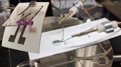
They evaluated both short- and longer-term performance in a special fixture (Fig. 2).
Prof. Franklin added that previous reports claim “all-carbon” electronics actually incorporate inorganic components, focusing only on a carbonaceous channel and electrodes. However, the printed CNC gate dielectric in their TFTs yields a truly all-carbon device that they dubbed “all-carbon recyclable electronics” (ACRE). They also compared performance of their printed device to others reported by other researchers (Fig. 3).
What about the recover/reuse considerations? By submerging their devices in a series of baths, gently vibrating them with sound waves, and centrifuging the resulting solution, the carbon nanotubes and graphene are sequentially recovered with an average yield of nearly 100%. Both materials may then be reused in the same printing process while losing very little of their performance viability, and the nanocellulose, being made from wood, can simply be recycled along with the paper on which it was printed (Fig. 4).
Franklin explained that by demonstrating a fully recyclable, multifunctional, printed transistor first, he hopes to make a first step toward the technology being commercially pursued for simple devices. For example, the technology could find a role in a large building needing thousands of simple environmental sensors to monitor its energy use, or in customized biosensing patches for tracking medical conditions.
Their published article in Nature Electronics “Printable and recyclable carbon electronics using crystalline nanocellulose dielectrics” is highly readable, discussing how they devised the idea and developed the specific inks, including the rationale, modifications, and testing of each (it’s behind a paywall but an open version is posted here). In addition, there’s a short video of the printing here. Furthermore, a “Supplementary Information” posting shows that the team has truly done its homework, as it presents a detailed table listing 28 other somewhat-similar projects with their reference citations, and the key technical attributes and specifications of each, to demonstrate why their approach is a distinct improvement. Perhaps, some day, “printed circuits” will truly be made that way?


