Implementing a Frequency Multiplier Using Mixed-Signal Programmable Devices
Members can download this article in PDF format.
What you’ll learn:
- How to implement a frequency multiplier.
- How to create circuit designs in the GreenPAK Designer software.
This article describes how to implement a frequency multiplier using a GreenPAK programmable mixed-signal IC. The frequency multiplier can be used in a range of applications, including control circuits and communication devices.
Terms and Definitions
- CD: Counter data
- CNT: Counter
- DCMP: Digital comparator
- FSM: Finite state machine
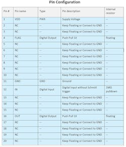
See the table below for the pin configuration.
The complete design file is available at this link. This circuit design was created in free GUI-based GreenPAK Designer software, a part of the Go Configure Software Hub package.
Design Overview
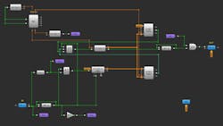
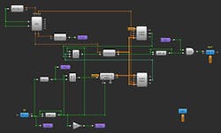
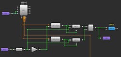
The overall GreenPAK design is shown in Figures 1 and 2.
The design can be divided into the following blocks:
- Frequency multiplier
- Selector
- Multiplier settings
- FLAG
- OUT
Frequency Multiplier
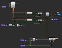
The design includes two frequency-multiplier blocks consisting of FSM0/DCMP0 and FSM1/ DCMP2, as shown in Figure 3.
The frequency-multiplier block that consists of FSM1/DCMP2 operates as follows: When the signal from the selector is LOW, then FSM1 counts the IN frequency, and when the signal from the selector is HIGH, then FSM1, CNT8, and DCMP2 generate an OUT frequency.
Selector
The selector chooses which of the two blocks counts input frequency and which generates the multiplied output frequency (Fig. 4).
Multiplier Settings
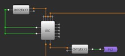
CNT3 is used to select a factor by which the input frequency is multiplied (Fig. 5). The counter data is determined by the formula:
CD = 2 * N − 1
where CD is counter data and N is the multiplying factor.
CNT7 is used to determine the input frequency. The counter period should be approximately:
T ≈ 1/(100 ∙ F ∙ N)
where T is the counter period, F is the approximate input frequency, and N is the multiplying factor.
FLAG
For a given input frequency the circuit multiplexer range is between 0.2x and 5x. If the frequency is outside of this range, then FLAG will be LOW (Fig. 6).
OUT
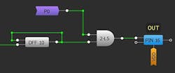
If FLAG is HIGH, DFF10 generates the output frequency with a 50% duty cycle. If FLAG is LOW, then OUT will be LOW (Fig. 7).
Example
In one example, consider multiplying an input frequency of ~1 kHz by a factor of 15. The counter data CNT3 should be:
CD = 2 * 15 – 1 = 29
The counter period of CNT7 should be:
T ≈ [1/(100 ∙ 1000 Hz ∙ 15)] ≈ 666 ns
Experimental Waveforms
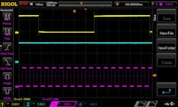
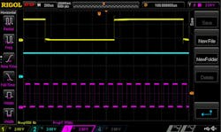
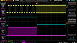
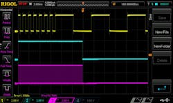
Figures 8 through 12 illustrate the experimental waveforms.
- Channel 1 (yellow/top line): PIN#12 (IN)
- Channel 2 (light blue/2nd line): PIN#4 (FLAG)
- Channel 3 (magenta/3rd line): PIN#16 (OUT)
Conclusion
This article demonstrates how to make a frequency multiplier using a GreenPAK IC. Only a few internal blocks of the SLG46620 chip are used, leaving the bulk of the blocks available to build other circuitry. The given design is limited to an input frequency range of 0.2x to 5x the typical frequency for which the circuit was debugged (~1 kHz). The typical output frequency can’t exceed 135 kHz.
Due to its size, configurability, and price, the GreenPAK provides an efficient and low-cost approach to implement a frequency multiplier.
